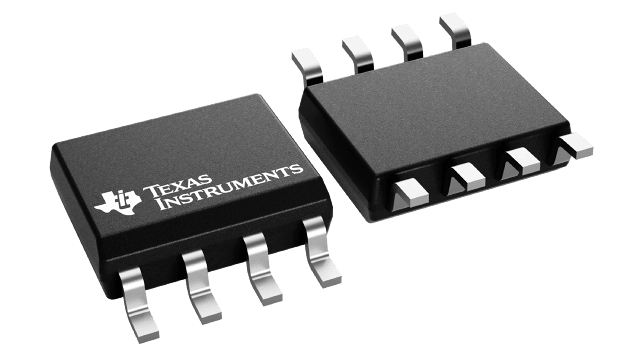
CDCVF2505IDRQ1
ActiveAUTOMOTIVE PLL CLOCK DRIVER FOR SYNCHRONIZATION, DRAM & GEN-PURPOSE APPS WITH SPREAD-SPECTRUM COMPAT
Deep-Dive with AI
Search across all available documentation for this part.

CDCVF2505IDRQ1
ActiveAUTOMOTIVE PLL CLOCK DRIVER FOR SYNCHRONIZATION, DRAM & GEN-PURPOSE APPS WITH SPREAD-SPECTRUM COMPAT
Deep-Dive with AI
Technical Specifications
Parameters and characteristics commom to parts in this series
| Specification | CDCVF2505IDRQ1 | CDCVF2505 Series |
|---|---|---|
| Differential - Input:Output [custom] | False | False |
| Differential - Input:Output [custom] | False | False |
| Divider/Multiplier [custom] | False | False |
| Divider/Multiplier [custom] | False | False |
| Frequency - Max [Max] | 200 MHz | 200 MHz |
| Grade | Automotive | Automotive |
| Mounting Type | Surface Mount | Surface Mount |
| Number of Circuits | 1 | 1 |
| Operating Temperature [Max] | 85 °C | 85 °C |
| Operating Temperature [Min] | -40 °C | -40 °C |
| Output | LVTTL | LVTTL |
| Package / Case | 3.9 mm | 3.9 mm |
| Package / Case | 8-SOIC | 8-TSSOP (0.173", 4.40mm Width), 8-SOIC |
| PLL | Yes with Bypass | Yes with Bypass |
| Qualification | AEC-Q100 | AEC-Q100 |
| Ratio - Input:Output [custom] | 1:5 | 1:5 |
| Supplier Device Package | 8-SOIC | 8-TSSOP, 8-SOIC |
| Type | PLL Clock Driver | PLL Clock Driver |
| Voltage - Supply [Max] | 3.6 V | 3.6 V |
| Voltage - Supply [Min] | 3 V | 3 V |
Pricing
Prices provided here are for design reference only. For realtime values and availability, please visit the distributors directly
| Distributor | Package | Quantity | $ | |
|---|---|---|---|---|
| Digikey | Cut Tape (CT) | 1 | $ 4.00 | |
| Digi-Reel® | 1 | $ 4.00 | ||
| Tape & Reel (TR) | 2500 | $ 2.01 | ||
| 5000 | $ 1.93 | |||
| Texas Instruments | LARGE T&R | 1 | $ 3.50 | |
| 100 | $ 3.07 | |||
| 250 | $ 2.15 | |||
| 1000 | $ 1.74 | |||
CDCVF2505 Series
PLL clock driver for synch. DRAM & gen. purp. apps w/spread spectrum compatibility, power down mode
| Part | Output | Ratio - Input:Output [custom] | Package / Case | Supplier Device Package | Number of Circuits | Differential - Input:Output [custom] | Differential - Input:Output [custom] | Divider/Multiplier [custom] | Divider/Multiplier [custom] | Mounting Type | Type | Operating Temperature [Min] | Operating Temperature [Max] | PLL | Voltage - Supply [Max] | Voltage - Supply [Min] | Frequency - Max [Max] | Package / Case | Grade | Qualification |
|---|---|---|---|---|---|---|---|---|---|---|---|---|---|---|---|---|---|---|---|---|
Texas Instruments CDCVF2505PW | LVTTL | 1:5 | 8-TSSOP (0.173", 4.40mm Width) | 8-TSSOP | 1 | Surface Mount | PLL Clock Driver | -40 °C | 85 °C | Yes with Bypass | 3.6 V | 3 V | 200 MHz | |||||||
Texas Instruments CDCVF2505DR | LVTTL | 1:5 | 8-SOIC | 8-SOIC | 1 | Surface Mount | PLL Clock Driver | -40 °C | 85 °C | Yes with Bypass | 3.6 V | 3 V | 200 MHz | 3.9 mm | ||||||
Texas Instruments CDCVF2505D | LVTTL | 1:5 | 8-SOIC | 8-SOIC | 1 | Surface Mount | PLL Clock Driver | -40 °C | 85 °C | Yes with Bypass | 3.6 V | 3 V | 200 MHz | 3.9 mm | ||||||
Texas Instruments CDCVF2505PWRG4 | LVTTL | 1:5 | 8-TSSOP (0.173", 4.40mm Width) | 8-TSSOP | 1 | Surface Mount | PLL Clock Driver | -40 °C | 85 °C | Yes with Bypass | 3.6 V | 3 V | 200 MHz | |||||||
Texas Instruments CDCVF2505PWR | LVTTL | 1:5 | 8-TSSOP (0.173", 4.40mm Width) | 8-TSSOP | 1 | Surface Mount | PLL Clock Driver | -40 °C | 85 °C | Yes with Bypass | 3.6 V | 3 V | 200 MHz | |||||||
Texas Instruments CDCVF2505DG4 | LVTTL | 1:5 | 8-SOIC | 8-SOIC | 1 | Surface Mount | PLL Clock Driver | -40 °C | 85 °C | Yes with Bypass | 3.6 V | 3 V | 200 MHz | 3.9 mm | ||||||
Texas Instruments CDCVF2505DRG4 | LVTTL | 1:5 | 8-SOIC | 8-SOIC | 1 | Surface Mount | PLL Clock Driver | -40 °C | 85 °C | Yes with Bypass | 3.6 V | 3 V | 200 MHz | 3.9 mm | ||||||
Texas Instruments CDCVF2505IDRQ1 | LVTTL | 1:5 | 8-SOIC | 8-SOIC | 1 | Surface Mount | PLL Clock Driver | -40 °C | 85 °C | Yes with Bypass | 3.6 V | 3 V | 200 MHz | 3.9 mm | Automotive | AEC-Q100 |
Description
General part information
CDCVF2505 Series
The CDCVF2505 is a high-performance, low-skew, low-jitter, phase-lock loop (PLL) clock driver. This device uses a PLL to precisely align the output clocks (1Y[0-3] and CLKOUT) to the input clock signal (CLKIN) in both frequency and phase. The CDCVF2505 operates at 3.3 V and also provides integrated series-damping resistors that make it ideal for driving point-to-point loads.
One bank of five outputs provides low-skew, low-jitter copies of CLKIN. Output duty cycles are adjusted to 50 percent, independent of duty cycle at CLKIN. The device automatically goes into power-down mode when no input signal is applied to CLKIN.
The loop filter for the PLLs is included on-chip. This minimizes the component count, space, and cost.
Documents
Technical documentation and resources


