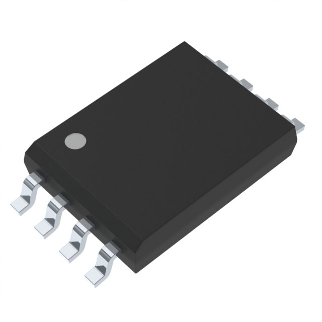
STGAP2HSM
ActiveIC: DRIVER; GATE DRIVER; SO8-W; -4÷4A; 1.2KV; CH: 1; USUP: 3.1÷5.5V
Deep-Dive with AI
Search across all available documentation for this part.

STGAP2HSM
ActiveIC: DRIVER; GATE DRIVER; SO8-W; -4÷4A; 1.2KV; CH: 1; USUP: 3.1÷5.5V
Deep-Dive with AI
Technical Specifications
Parameters and characteristics for this part
| Specification | STGAP2HSM |
|---|---|
| Approval Agency | UL |
| Common Mode Transient Immunity (Min) [Min] | 100 V/ns |
| Current - Output High, Low [custom] | 4 A |
| Current - Output High, Low [custom] | 4 A |
| Current - Peak Output | 4 A |
| Mounting Type | Surface Mount |
| Number of Channels | 1 |
| Operating Temperature [Max] | 125 °C |
| Operating Temperature [Min] | -40 °C |
| Package / Case | 8-SOIC |
| Package / Case [custom] | 0.295 in |
| Package / Case [custom] | 7.5 mm |
| Propagation Delay tpLH / tpHL (Max) [custom] | 90 ns |
| Propagation Delay tpLH / tpHL (Max) [custom] | 90 ns |
| Pulse Width Distortion (Max) [Max] | 20 ns |
| Rise / Fall Time (Typ) [custom] | 30 ns |
| Rise / Fall Time (Typ) [custom] | 30 ns |
| Supplier Device Package | 8-SO |
| Technology | Capacitive Coupling |
| Voltage - Output Supply [Max] | 5.5 V |
| Voltage - Output Supply [Min] | 3 V |
Pricing
Prices provided here are for design reference only. For realtime values and availability, please visit the distributors directly
Description
General part information
STGAP2SICSN Series
The STGAP2SICSN is a single gate driver which provides galvanic isolation between the gate driving channel and the low voltage control and interface circuitry.
The gate driver is characterized by 4 A capability and rail-to-rail outputs, making the device also suitable for mid and high power applications such as power conversion and motor driver inverters in industrial applications. The device is available in two different configurations. The configuration with separated output pins allows to independently optimize turn-on and turn-off by using dedicated gate resistors. The configuration featuring single output pin and Miller CLAMP function prevents gate spikes during fast commutations in half-bridge topologies. Both configurations provide high flexibility and bill of material reduction for external components.
The device integrates protection functions: UVLO with optimized value for SiC MOSFETs and thermal shutdown are included to easily design high reliability systems. Dual input pins allow choosing the control signal polarity and also implementing HW interlocking protection in order to avoid cross-conduction in case of controller malfunction. The input to output propagation delay results are contained within 75 ns, providing high PWM control accuracy. A standby mode is available in order to reduce idle power consumption.
Documents
Technical documentation and resources
No documents available


