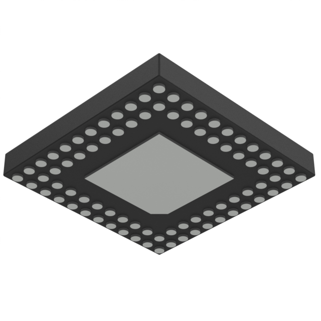
PI6CB332001AZXBIEX-13R
Active20-OUTPUT PCIE 4.0/5.0/6.0 CLOCK BUFFER WITH ON-CHIP TERMINATION
Deep-Dive with AI
Search across all available documentation for this part.

PI6CB332001AZXBIEX-13R
Active20-OUTPUT PCIE 4.0/5.0/6.0 CLOCK BUFFER WITH ON-CHIP TERMINATION
Deep-Dive with AI
Technical Specifications
Parameters and characteristics for this part
| Specification | PI6CB332001AZXBIEX-13R |
|---|---|
| Differential - Input:Output [custom] | True |
| Differential - Input:Output [custom] | True |
| Frequency - Max [Max] | 400 MHz |
| Input | HCSL, CMOS |
| Mounting Type | Surface Mount |
| Number of Circuits | 1 |
| Operating Temperature [Max] | 85 °C |
| Operating Temperature [Min] | -40 °C |
| Output | HCSL |
| Package / Case | 80-VFQFN Dual Rows, Exposed Pad |
| Ratio - Input:Output [custom] | 1:20 |
| Supplier Device Package | 80-aQFN (6x6) |
| Type | Clock Buffer |
| Voltage - Supply [Max] | 3.465 V |
| Voltage - Supply [Min] | 3.135 V |
Pricing
Prices provided here are for design reference only. For realtime values and availability, please visit the distributors directly
| Distributor | Package | Quantity | $ | |
|---|---|---|---|---|
| Digikey | Tape & Reel (TR) | 3000 | $ 6.30 | |
Description
General part information
PI6CB332001A Series
The PI6CB332001A is a 20-output, very low-power, PCIe® 1.0/2.0/3.0/4.0/5.0/6.0 clock buffer. The device is capable of distributing the reference clocks for UPI, SAS, SATA, and other applications. It takes a reference input to fanout twenty 100MHz low-power differential HCSL outputs with on-chip terminations. The on-chip termination can save 80 external resistors and make layout easier. OE pins combined with SMBus bits, as well as a 3-wire side band interface, provide easier power management for each output. All OE pins are power down tolerant, which allows the OE pins to be driven by external signals when the device is in a power down or reset condition. The device must reset and power up properly if these pins are driven to any valid voltage prior to the assertion of VDD or PWRGD#.
Documents
Technical documentation and resources


