TPS22975EVM
ActiveEVALUATION MODULE
Deep-Dive with AI
Search across all available documentation for this part.
TPS22975EVM
ActiveEVALUATION MODULE
Deep-Dive with AI
Technical Specifications
Parameters and characteristics commom to parts in this series
| Specification | TPS22975EVM | TPS22975 Series |
|---|---|---|
| Current - Output (Max) | - | 6 A |
| Fault Protection | - | Over Temperature |
| Features | - | Slew Rate Controlled, Load Discharge |
| Function | Power Distribution Switch (Load Switch) | Power Distribution Switch (Load Switch) |
| Input Type | - | Non-Inverting |
| Interface | - | On/Off |
| Mounting Type | - | Surface Mount |
| Number of Outputs | - | 1 |
| Operating Temperature | - | 105 °C |
| Operating Temperature | - | -40 °C |
| Output Configuration | - | High Side |
| Output Type | - | N-Channel |
| Package / Case | - | 8-WFDFN Exposed Pad |
| Ratio - Input:Output | - | 1:1 |
| Rds On (Typ) | - | 16 mOhm |
| Supplied Contents | Board(s) | Board(s) |
| Supplier Device Package | - | 8-WSON (2x2) |
| Switch Type | - | General Purpose |
| Type | Power Management | Power Management |
| Utilized IC / Part | TPS22975 | TPS22975 |
| Voltage - Load | - | 5.7 V |
| Voltage - Load | - | 2.5 V |
| Voltage - Supply (Vcc/Vdd) | - | Not Required |
Pricing
Prices provided here are for design reference only. For realtime values and availability, please visit the distributors directly
TPS22975 Series
5.7-V, 6-A, 16-mΩ load switch with adj. rise time, optional output discharge, and thermal shutdown
| Part | Mounting Type | Voltage - Supply (Vcc/Vdd) | Output Configuration | Features | Ratio - Input:Output [custom] | Fault Protection | Supplier Device Package | Current - Output (Max) [Max] | Input Type | Rds On (Typ) [custom] | Number of Outputs | Interface | Package / Case | Output Type | Switch Type | Operating Temperature [Max] | Operating Temperature [Min] | Voltage - Load [Max] | Voltage - Load [Min] | Type | Utilized IC / Part | Function | Supplied Contents |
|---|---|---|---|---|---|---|---|---|---|---|---|---|---|---|---|---|---|---|---|---|---|---|---|
Texas Instruments TPS22975NDSGTThe TPS22975 product family consists of two devices: TPS22975 and TPS22975N. Each device is a single-channel load switch that provides a configurable rise time to minimize inrush current. The device contains an N-channel MOSFET that can operate over an input voltage range of 0.6 V to 5.7 V and can support a maximum continuous current of 6 A. The switch is controlled by an on and off input (ON), which is capable of interfacing directly with low-voltage control signals. TPS22975 has an optional 230-Ω on-chip load resistor for quick output discharge when switch is turned off.
The TPS22975 is available in a small, space-saving 2-mm × 2-mm 8-pin SON package (DSG) with integrated thermal pad allowing for high power dissipation. The device is characterized for operation over the free-air temperature range of –40°C to +105°C.
The TPS22975 product family consists of two devices: TPS22975 and TPS22975N. Each device is a single-channel load switch that provides a configurable rise time to minimize inrush current. The device contains an N-channel MOSFET that can operate over an input voltage range of 0.6 V to 5.7 V and can support a maximum continuous current of 6 A. The switch is controlled by an on and off input (ON), which is capable of interfacing directly with low-voltage control signals. TPS22975 has an optional 230-Ω on-chip load resistor for quick output discharge when switch is turned off.
The TPS22975 is available in a small, space-saving 2-mm × 2-mm 8-pin SON package (DSG) with integrated thermal pad allowing for high power dissipation. The device is characterized for operation over the free-air temperature range of –40°C to +105°C. | Surface Mount | Not Required | High Side | Slew Rate Controlled | 1:1 | Over Temperature | 8-WSON (2x2) | 6 A | Non-Inverting | 16 mOhm | 1 | On/Off | 8-WFDFN Exposed Pad | N-Channel | General Purpose | 105 °C | -40 °C | 5.7 V | 2.5 V | ||||
Texas Instruments TPS22975NDSGRThe TPS22975 product family consists of two devices: TPS22975 and TPS22975N. Each device is a single-channel load switch that provides a configurable rise time to minimize inrush current. The device contains an N-channel MOSFET that can operate over an input voltage range of 0.6 V to 5.7 V and can support a maximum continuous current of 6 A. The switch is controlled by an on and off input (ON), which is capable of interfacing directly with low-voltage control signals. TPS22975 has an optional 230-Ω on-chip load resistor for quick output discharge when switch is turned off.
The TPS22975 is available in a small, space-saving 2-mm × 2-mm 8-pin SON package (DSG) with integrated thermal pad allowing for high power dissipation. The device is characterized for operation over the free-air temperature range of –40°C to +105°C.
The TPS22975 product family consists of two devices: TPS22975 and TPS22975N. Each device is a single-channel load switch that provides a configurable rise time to minimize inrush current. The device contains an N-channel MOSFET that can operate over an input voltage range of 0.6 V to 5.7 V and can support a maximum continuous current of 6 A. The switch is controlled by an on and off input (ON), which is capable of interfacing directly with low-voltage control signals. TPS22975 has an optional 230-Ω on-chip load resistor for quick output discharge when switch is turned off.
The TPS22975 is available in a small, space-saving 2-mm × 2-mm 8-pin SON package (DSG) with integrated thermal pad allowing for high power dissipation. The device is characterized for operation over the free-air temperature range of –40°C to +105°C. | Surface Mount | Not Required | High Side | Slew Rate Controlled | 1:1 | Over Temperature | 8-WSON (2x2) | 6 A | Non-Inverting | 16 mOhm | 1 | On/Off | 8-WFDFN Exposed Pad | N-Channel | General Purpose | 105 °C | -40 °C | 5.7 V | 2.5 V | ||||
Texas Instruments TPS22975DSGRThe TPS22975 product family consists of two devices: TPS22975 and TPS22975N. Each device is a single-channel load switch that provides a configurable rise time to minimize inrush current. The device contains an N-channel MOSFET that can operate over an input voltage range of 0.6 V to 5.7 V and can support a maximum continuous current of 6 A. The switch is controlled by an on and off input (ON), which is capable of interfacing directly with low-voltage control signals. TPS22975 has an optional 230-Ω on-chip load resistor for quick output discharge when switch is turned off.
The TPS22975 is available in a small, space-saving 2-mm × 2-mm 8-pin SON package (DSG) with integrated thermal pad allowing for high power dissipation. The device is characterized for operation over the free-air temperature range of –40°C to +105°C.
The TPS22975 product family consists of two devices: TPS22975 and TPS22975N. Each device is a single-channel load switch that provides a configurable rise time to minimize inrush current. The device contains an N-channel MOSFET that can operate over an input voltage range of 0.6 V to 5.7 V and can support a maximum continuous current of 6 A. The switch is controlled by an on and off input (ON), which is capable of interfacing directly with low-voltage control signals. TPS22975 has an optional 230-Ω on-chip load resistor for quick output discharge when switch is turned off.
The TPS22975 is available in a small, space-saving 2-mm × 2-mm 8-pin SON package (DSG) with integrated thermal pad allowing for high power dissipation. The device is characterized for operation over the free-air temperature range of –40°C to +105°C. | Surface Mount | Not Required | High Side | Load Discharge, Slew Rate Controlled | 1:1 | Over Temperature | 8-WSON (2x2) | 6 A | Non-Inverting | 16 mOhm | 1 | On/Off | 8-WFDFN Exposed Pad | N-Channel | General Purpose | 105 °C | -40 °C | 5.7 V | 2.5 V | ||||
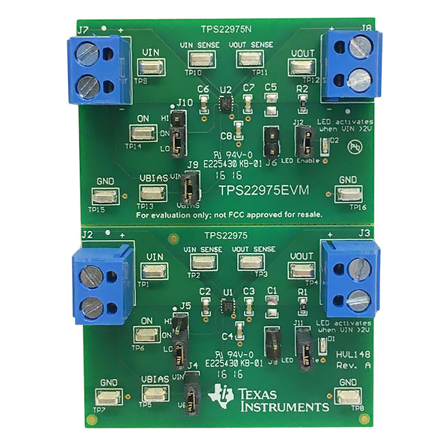
Texas Instruments TPS22975EVMTPS22975 Power Distribution Switch (Load Switch) Power Management Evaluation Board | Power Management | TPS22975 | Power Distribution Switch (Load Switch) | Board(s) | |||||||||||||||||||
Texas Instruments TPS22975DSGTThe TPS22975 product family consists of two devices: TPS22975 and TPS22975N. Each device is a single-channel load switch that provides a configurable rise time to minimize inrush current. The device contains an N-channel MOSFET that can operate over an input voltage range of 0.6 V to 5.7 V and can support a maximum continuous current of 6 A. The switch is controlled by an on and off input (ON), which is capable of interfacing directly with low-voltage control signals. TPS22975 has an optional 230-Ω on-chip load resistor for quick output discharge when switch is turned off.
The TPS22975 is available in a small, space-saving 2-mm × 2-mm 8-pin SON package (DSG) with integrated thermal pad allowing for high power dissipation. The device is characterized for operation over the free-air temperature range of –40°C to +105°C.
The TPS22975 product family consists of two devices: TPS22975 and TPS22975N. Each device is a single-channel load switch that provides a configurable rise time to minimize inrush current. The device contains an N-channel MOSFET that can operate over an input voltage range of 0.6 V to 5.7 V and can support a maximum continuous current of 6 A. The switch is controlled by an on and off input (ON), which is capable of interfacing directly with low-voltage control signals. TPS22975 has an optional 230-Ω on-chip load resistor for quick output discharge when switch is turned off.
The TPS22975 is available in a small, space-saving 2-mm × 2-mm 8-pin SON package (DSG) with integrated thermal pad allowing for high power dissipation. The device is characterized for operation over the free-air temperature range of –40°C to +105°C. | Surface Mount | Not Required | High Side | Load Discharge, Slew Rate Controlled | 1:1 | Over Temperature | 8-WSON (2x2) | 6 A | Non-Inverting | 16 mOhm | 1 | On/Off | 8-WFDFN Exposed Pad | N-Channel | General Purpose | 105 °C | -40 °C | 5.7 V | 2.5 V |
Description
General part information
TPS22975 Series
The TPS22975 product family consists of two devices: TPS22975 and TPS22975N. Each device is a single-channel load switch that provides a configurable rise time to minimize inrush current. The device contains an N-channel MOSFET that can operate over an input voltage range of 0.6 V to 5.7 V and can support a maximum continuous current of 6 A. The switch is controlled by an on and off input (ON), which is capable of interfacing directly with low-voltage control signals. TPS22975 has an optional 230-Ω on-chip load resistor for quick output discharge when switch is turned off.
The TPS22975 is available in a small, space-saving 2-mm × 2-mm 8-pin SON package (DSG) with integrated thermal pad allowing for high power dissipation. The device is characterized for operation over the free-air temperature range of –40°C to +105°C.
The TPS22975 product family consists of two devices: TPS22975 and TPS22975N. Each device is a single-channel load switch that provides a configurable rise time to minimize inrush current. The device contains an N-channel MOSFET that can operate over an input voltage range of 0.6 V to 5.7 V and can support a maximum continuous current of 6 A. The switch is controlled by an on and off input (ON), which is capable of interfacing directly with low-voltage control signals. TPS22975 has an optional 230-Ω on-chip load resistor for quick output discharge when switch is turned off.
Documents
Technical documentation and resources