Zenode.ai Logo
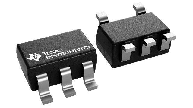
SOT-23 (DBV)

CLVC1G125QDBVRQ1

Active
Texas Instruments

AUTOMOTIVE SINGLE 1.65-V TO 5.5-V BUFFER WITH 3-STATE OUTPUTS

Find alt
SOT-23 (DBV)

CLVC1G125QDBVRQ1

Active
Texas Instruments

AUTOMOTIVE SINGLE 1.65-V TO 5.5-V BUFFER WITH 3-STATE OUTPUTS

Find alt

Description

General part information

SN74LVC1G125-Q1 Series

This bus buffer gate is designed for 1.65-V to 5.5-V VCCoperation.

The SN74LVC1G125-Q1 device is a single line driver with a 3-state output. The output is disabled when the output-enable (OE) input is high.

The CMOS device has high output drive while maintaining low static power dissipation over a broad VCCoperating range.

Technical Specifications

Parameters and characteristics for this part

SpecificationCLVC1G125QDBVRQ1
Current - Output High24 mA
Current - Output Low24 mA
GradeAutomotive
Logic TypeBuffer, Non-Inverting
Mounting TypeSurface Mount
Number of Bits per Element1 bits
Number of Elements1
Operating Temperature (Max)125 °C
Operating Temperature (Min)-40 °C
Output Type3-State
Package NameSOT-23-5
QualificationAEC-Q100
Voltage - Supply (Maximum)5.5 V
Voltage - Supply (Minimum)1.65 V

Pricing

Prices provided here are for design reference only. For realtime values and availability, please visit the distributors directly

Sign in to see pricing

Create a free account to access distributor pricing data.

CAD

3D models and CAD resources for this part

Documents

Technical documentation and resources

Datasheet
STANDARD LINEAR AND LOGIC FOR DVD/VCD PLAYERS
16-Bit Widebus Logic Families in 56-Ball, 0.65-mm Pitch Very Thin Fine-Pitch BGA (Rev. B)
Understanding Advanced Bus-Interface Products Design Guide
Understanding and Interpreting Standard-Logic Data Sheets (Rev. C)
Optimizing On-Board and Wireless Charger Systems Using Logic and Translation (Rev. A)
LVC Characterization Information
Drive Transmission Lines With Logic
LOGIC Pocket Data Book (Rev. B)
Low-Voltage Logic (LVC) Designer's Guide
Texas Instruments Little Logic Application Report
Little Logic Guide 2018 (Rev. G)
Implications of Slow or Floating CMOS Inputs (Rev. E)
Automotive Logic Devices Brochure
Migration From 3.3-V To 2.5-V Power Supplies For Logic Devices
Selecting the Right Level Translation Solution (Rev. A)
Bus-Interface Devices With Output-Damping Resistors Or Reduced-Drive Outputs (Rev. A)
LVC and LV Low-Voltage CMOS Logic Data Book (Rev. B)
Logic Guide (Rev. AB)
SN74LVC1G125-Q1 Single-BUS buffer gate with 3-state output datasheet (Rev. E)
Standard Linear & Logic for PCs, Servers & Motherboards
CMOS Power Consumption and CPD Calculation (Rev. B)
Signal Switch Data Book (Rev. A)
Semiconductor Packing Material Electrostatic Discharge (ESD) Protection
TI IBIS File Creation, Validation, and Distribution Processes
Live Insertion
Design Summary for WCSP Little Logic (Rev. B)
Use of the CMOS Unbuffered Inverter in Oscillator Circuits
Power-Up 3-State (PU3S) Circuits in TI Standard Logic Devices
How to Select Little Logic (Rev. A)
Input and Output Characteristics of Digital Integrated Circuits