ADC3444IRTQR
ActiveQUAD-CHANNEL, 14-BIT, 125-MSPS ANALOG-TO-DIGITAL CONVERTER (ADC)
Deep-Dive with AI
Search across all available documentation for this part.
ADC3444IRTQR
ActiveQUAD-CHANNEL, 14-BIT, 125-MSPS ANALOG-TO-DIGITAL CONVERTER (ADC)
Technical Specifications
Parameters and characteristics commom to parts in this series
| Specification | ADC3444IRTQR | ADC3444 Series |
|---|---|---|
| Architecture | Pipelined | Pipelined |
| Configuration | ADC | ADC |
| Data Interface | LVDS - Serial | LVDS - Serial |
| Features | - | Simultaneous Sampling |
| Input Range | - | 2 Vpp |
| Input Type | Differential | Differential |
| Mounting Type | Surface Mount | Surface Mount |
| Number of A/D Converters | 4 | 4 |
| Number of Bits | 14 | 14 |
| Number of Inputs | 4 | 4 |
| Operating Temperature [Max] | 85 °C | 85 °C |
| Operating Temperature [Min] | -40 °C | -40 °C |
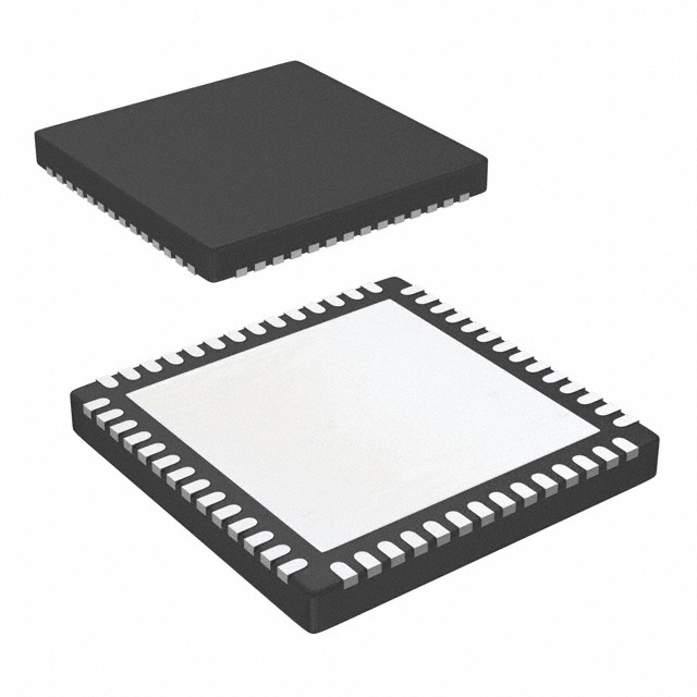
| Package / Case | 56-VFQFN Exposed Pad | 56-VFQFN Exposed Pad |
| Power (Typ) @ Conditions | - | 391 mW |
| Ratio - S/H:ADC | 0:1 | 0:1 |
| Reference Type | Internal, External | Internal, External |
| Sampling Rate (Per Second) | 125 M | 125 M |
| Supplied Contents | - | Board(s) |
| Supplier Device Package | 56-QFN (8x8) | 56-QFN (8x8) |
| Utilized IC / Part | - | ADC3444 |
| Voltage - Supply, Analog [Max] | 1.9 V | 1.9 V |
| Voltage - Supply, Analog [Min] | 1.7 V | 1.7 V |
| Voltage - Supply, Digital [Max] | 1.9 V | 1.9 V |
| Voltage - Supply, Digital [Min] | 1.7 V | 1.7 V |
Pricing
Prices provided here are for design reference only. For realtime values and availability, please visit the distributors directly
ADC3444 Series
Quad-Channel, 14-Bit, 125-MSPS Analog-to-Digital Converter (ADC)
| Part | Input Type | Sampling Rate (Per Second) | Voltage - Supply, Digital [Min] | Voltage - Supply, Digital [Max] | Supplier Device Package | Data Interface | Features | Voltage - Supply, Analog [Min] | Voltage - Supply, Analog [Max] | Operating Temperature [Min] | Operating Temperature [Max] | Architecture | Number of A/D Converters | Number of Bits | Configuration | Number of Inputs | Package / Case | Reference Type | Mounting Type | Input Range | Power (Typ) @ Conditions | Utilized IC / Part | Supplied Contents | Ratio - S/H:ADC |
|---|---|---|---|---|---|---|---|---|---|---|---|---|---|---|---|---|---|---|---|---|---|---|---|---|
Texas Instruments ADC3444IRTQTThe ADC344x devices are a high-linearity, ultra-low power, quad-channel, 14-bit, 25-MSPS to 125-MSPS, analog-to-digital converter (ADC) family. The devices are designed specifically to support demanding, high input frequency signals with large dynamic range requirements. An input clock divider allows more flexibility for system clock architecture design while the SYSREF input enables complete system synchronization.
The ADC344x family supports serial low-voltage differential signaling (LVDS) to reduce the number of interface lines, thus allowing for high system integration density. The serial LVDS interface is two-wire, where each ADC data are serialized and output over two LVDS pairs. Optionally, a one-wire serial LVDS interface is available. An internal phase-locked loop (PLL) multiplies the incoming ADC sampling clock to derive the bit clock that is used to serialize the 14-bit output data from each channel. In addition to the serial data streams, the frame and bit clocks are transmitted as LVDS outputs.
The ADC344x devices are a high-linearity, ultra-low power, quad-channel, 14-bit, 25-MSPS to 125-MSPS, analog-to-digital converter (ADC) family. The devices are designed specifically to support demanding, high input frequency signals with large dynamic range requirements. An input clock divider allows more flexibility for system clock architecture design while the SYSREF input enables complete system synchronization.
The ADC344x family supports serial low-voltage differential signaling (LVDS) to reduce the number of interface lines, thus allowing for high system integration density. The serial LVDS interface is two-wire, where each ADC data are serialized and output over two LVDS pairs. Optionally, a one-wire serial LVDS interface is available. An internal phase-locked loop (PLL) multiplies the incoming ADC sampling clock to derive the bit clock that is used to serialize the 14-bit output data from each channel. In addition to the serial data streams, the frame and bit clocks are transmitted as LVDS outputs. | Differential | 125 M | 1.7 V | 1.9 V | 56-QFN (8x8) | LVDS - Serial | Simultaneous Sampling | 1.7 V | 1.9 V | -40 °C | 85 °C | Pipelined | 4 | 14 | ADC | 4 | 56-VFQFN Exposed Pad | External, Internal | Surface Mount | |||||
Texas Instruments ADC3444EVMADC3444 - 14 Bit 125M Samples per Second Analog to Digital Converter (ADC) Evaluation Board | 125 M | LVDS - Serial | 4 | 14 | 2 Vpp | 391 mW | ADC3444 | Board(s) | ||||||||||||||||
Texas Instruments ADC3444IRTQRThe ADC344x devices are a high-linearity, ultra-low power, quad-channel, 14-bit, 25-MSPS to 125-MSPS, analog-to-digital converter (ADC) family. The devices are designed specifically to support demanding, high input frequency signals with large dynamic range requirements. An input clock divider allows more flexibility for system clock architecture design while the SYSREF input enables complete system synchronization.
The ADC344x family supports serial low-voltage differential signaling (LVDS) to reduce the number of interface lines, thus allowing for high system integration density. The serial LVDS interface is two-wire, where each ADC data are serialized and output over two LVDS pairs. Optionally, a one-wire serial LVDS interface is available. An internal phase-locked loop (PLL) multiplies the incoming ADC sampling clock to derive the bit clock that is used to serialize the 14-bit output data from each channel. In addition to the serial data streams, the frame and bit clocks are transmitted as LVDS outputs.
The ADC344x devices are a high-linearity, ultra-low power, quad-channel, 14-bit, 25-MSPS to 125-MSPS, analog-to-digital converter (ADC) family. The devices are designed specifically to support demanding, high input frequency signals with large dynamic range requirements. An input clock divider allows more flexibility for system clock architecture design while the SYSREF input enables complete system synchronization.
The ADC344x family supports serial low-voltage differential signaling (LVDS) to reduce the number of interface lines, thus allowing for high system integration density. The serial LVDS interface is two-wire, where each ADC data are serialized and output over two LVDS pairs. Optionally, a one-wire serial LVDS interface is available. An internal phase-locked loop (PLL) multiplies the incoming ADC sampling clock to derive the bit clock that is used to serialize the 14-bit output data from each channel. In addition to the serial data streams, the frame and bit clocks are transmitted as LVDS outputs. | Differential | 125 M | 1.7 V | 1.9 V | 56-QFN (8x8) | LVDS - Serial | 1.7 V | 1.9 V | -40 °C | 85 °C | Pipelined | 4 | 14 | ADC | 4 | 56-VFQFN Exposed Pad | External, Internal | Surface Mount | 0:1 |
Description
General part information
ADC3444 Series
The ADC344x devices are a high-linearity, ultra-low power, quad-channel, 14-bit, 25-MSPS to 125-MSPS, analog-to-digital converter (ADC) family. The devices are designed specifically to support demanding, high input frequency signals with large dynamic range requirements. An input clock divider allows more flexibility for system clock architecture design while the SYSREF input enables complete system synchronization.
The ADC344x family supports serial low-voltage differential signaling (LVDS) to reduce the number of interface lines, thus allowing for high system integration density. The serial LVDS interface is two-wire, where each ADC data are serialized and output over two LVDS pairs. Optionally, a one-wire serial LVDS interface is available. An internal phase-locked loop (PLL) multiplies the incoming ADC sampling clock to derive the bit clock that is used to serialize the 14-bit output data from each channel. In addition to the serial data streams, the frame and bit clocks are transmitted as LVDS outputs.
The ADC344x devices are a high-linearity, ultra-low power, quad-channel, 14-bit, 25-MSPS to 125-MSPS, analog-to-digital converter (ADC) family. The devices are designed specifically to support demanding, high input frequency signals with large dynamic range requirements. An input clock divider allows more flexibility for system clock architecture design while the SYSREF input enables complete system synchronization.
Documents
Technical documentation and resources