DAC5681IRGCR
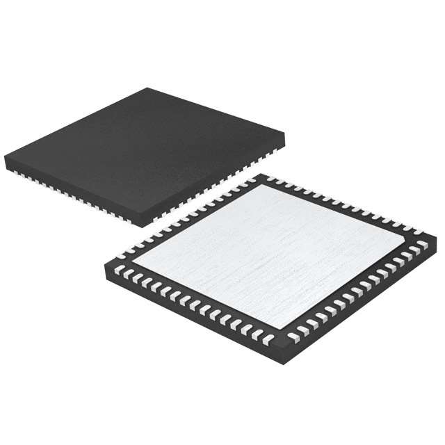
Active16-BIT, 1.0-GSPS DIGITAL-TO-ANALOG CONVERTER (DAC) 64-VQFN -40 TO 85
Deep-Dive with AI
Search across all available documentation for this part.
DAC5681IRGCR
Active16-BIT, 1.0-GSPS DIGITAL-TO-ANALOG CONVERTER (DAC) 64-VQFN -40 TO 85
Deep-Dive with AI
Technical Specifications
Parameters and characteristics commom to parts in this series
| Specification | DAC5681IRGCR | DAC5681 Series |
|---|---|---|
| Architecture | Current Sink | Current Sink |
| DAC Type | - | Current |
| Data Interface | LVDS - Parallel | LVDS - Parallel, LVDS - Serial |
| Differential Output | True | True |
| INL/DNL (LSB) | ±4, ±2 | ±4, ±2 |
| Mounting Type | Surface Mount | Surface Mount |
| Number of Bits | 16 bits | 16 bits |
| Number of DAC's | - | 1 |
| Operating Temperature [Max] | 85 °C | 85 °C |
| Operating Temperature [Min] | -40 °C | -40 °C |
| Output Type | Current - Unbuffered | Current - Unbuffered |
| Package / Case | 64-VFQFN Exposed Pad | 64-VFQFN Exposed Pad |
| Reference Type | Internal, External | Internal, External |
| Sampling Rate (Per Second) | - | 1 G |
| Settling Time | 10.4 ns | 10.4 ns |
| Supplied Contents | - | Board(s) |
| Supplier Device Package | 64-VQFN (9x9) | 64-VQFN (9x9) |
| Utilized IC / Part | - | DAC5681Z |
| Voltage - Supply, Analog [Max] | 3.6 V | 3.6 V |
| Voltage - Supply, Analog [Min] | 3 V | 3 V |
| Voltage - Supply, Digital [Max] | 2.15 V | 1.9 - 2.15 V |
| Voltage - Supply, Digital [Min] | 1.71 V | 1.7 - 1.71 V |
Pricing
Prices provided here are for design reference only. For realtime values and availability, please visit the distributors directly
DAC5681 Series
16-Bit, 1.0-GSPS Digital-to-Analog Converter (DAC)
| Part | Sampling Rate (Per Second) | Data Interface | Utilized IC / Part | Supplied Contents | Settling Time | DAC Type | Number of Bits | Number of DAC's | Output Type | Voltage - Supply, Digital [Max] | Voltage - Supply, Digital [Min] | Package / Case | Differential Output | Mounting Type | INL/DNL (LSB) | Supplier Device Package | Operating Temperature [Min] | Operating Temperature [Max] | Reference Type | Architecture | Voltage - Supply, Analog [Max] | Voltage - Supply, Analog [Min] |
|---|---|---|---|---|---|---|---|---|---|---|---|---|---|---|---|---|---|---|---|---|---|---|
Texas Instruments DAC5681ZEVMDAC5681Z 16 Bit 1G Samples Per Second Digital to Analog Converter (DAC) Evaluation Board | 1 G | LVDS - Parallel, LVDS - Serial | DAC5681Z | Board(s) | 10.4 ns | Current | 16 bits | 1 | ||||||||||||||
LVDS - Parallel | 10.4 ns | 16 bits | Current - Unbuffered | 2.15 V | 1.71 V | 64-VFQFN Exposed Pad | Surface Mount | ±2, ±4 | 64-VQFN (9x9) | -40 °C | 85 °C | External, Internal | Current Sink | 3.6 V | 3 V | |||||||
Texas Instruments DAC5681IRGCTThe DAC5681 is a 16-bit 1.0 GSPS digital-to-analog converter (DAC) with wideband LVDS data input and internal voltage reference. The DAC5681 offers superior linearity and noise performance.
The DAC5681 integrates a wideband LVDS port with on-chip termination, providing full 1.0 GSPS data transfer into the DAC and lower EMI than traditional CMOS data interfaces. An on-chip delay lock loop (DLL) simplifies LVDS interfacing by providing skew control for the LVDS input data clock.
The current-steering architecture of the DAC5681 consists of a segmented array of current sinking switches directing up to 20mA of full-scale current to complementary output nodes. An accurate on-chip voltage reference is temperature-compensated and delivers a stable 1.2-V reference voltage. Optionally, an external reference may be used.
The DAC5681 is characterized for operation over the industrial temperature range of –40°C to 85°C and is available in a 64-pin QFN package. The device is pin upgradeable to the other members of the family: the DAC5681Z and DAC5682Z. The single-channel DAC5681Z and dual-channel DAC5682Z both provide optional 2x/4x interpolation and a clock multiplying PLL.
The DAC5681 is a 16-bit 1.0 GSPS digital-to-analog converter (DAC) with wideband LVDS data input and internal voltage reference. The DAC5681 offers superior linearity and noise performance.
The DAC5681 integrates a wideband LVDS port with on-chip termination, providing full 1.0 GSPS data transfer into the DAC and lower EMI than traditional CMOS data interfaces. An on-chip delay lock loop (DLL) simplifies LVDS interfacing by providing skew control for the LVDS input data clock.
The current-steering architecture of the DAC5681 consists of a segmented array of current sinking switches directing up to 20mA of full-scale current to complementary output nodes. An accurate on-chip voltage reference is temperature-compensated and delivers a stable 1.2-V reference voltage. Optionally, an external reference may be used.
The DAC5681 is characterized for operation over the industrial temperature range of –40°C to 85°C and is available in a 64-pin QFN package. The device is pin upgradeable to the other members of the family: the DAC5681Z and DAC5682Z. The single-channel DAC5681Z and dual-channel DAC5682Z both provide optional 2x/4x interpolation and a clock multiplying PLL. | LVDS - Parallel | 10.4 ns | 16 bits | Current - Unbuffered | 2.15 V | 1.71 V | 64-VFQFN Exposed Pad | Surface Mount | ±2, ±4 | 64-VQFN (9x9) | -40 °C | 85 °C | External, Internal | Current Sink | 3.6 V | 3 V | ||||||
Texas Instruments DAC5681ZIRGCTThe DAC5681Z is a 16-bit 1.0 GSPS digital-to-analog converter (DAC) with wideband LVDS data input, integrated 2x to 4x interpolation filters, on-board clock multiplier, and internal voltage reference. The DAC5681Z offers superior linearity, noise, crosstalk, and PLL phase noise performance.
The DAC5681Z integrates a wideband LVDS port with on-chip termination. Full-rate input data can be transferred to a single DAC channel, or half-rate and 1/4-rate input data can be interpolated by on-board 2x or 4x FIR filters. Each interpolation FIR is configurable in either low-pass or high-pass mode, allowing selection of a higher order output spectral image. An on-chip delay lock loop (DLL) simplifies LVDS interfacing by providing skew control for the LVDS input data clock.
The DAC5681Z is characterized for operation over the industrial temperature range of –40°C to 85°C and is available in a 64-pin VQFN package. Other members of the family include the dual-channel, interpolating DAC5682Z and the single-channel, non-interpolating DAC5681.
The DAC5681Z is a 16-bit 1.0 GSPS digital-to-analog converter (DAC) with wideband LVDS data input, integrated 2x to 4x interpolation filters, on-board clock multiplier, and internal voltage reference. The DAC5681Z offers superior linearity, noise, crosstalk, and PLL phase noise performance.
The DAC5681Z integrates a wideband LVDS port with on-chip termination. Full-rate input data can be transferred to a single DAC channel, or half-rate and 1/4-rate input data can be interpolated by on-board 2x or 4x FIR filters. Each interpolation FIR is configurable in either low-pass or high-pass mode, allowing selection of a higher order output spectral image. An on-chip delay lock loop (DLL) simplifies LVDS interfacing by providing skew control for the LVDS input data clock.
The DAC5681Z is characterized for operation over the industrial temperature range of –40°C to 85°C and is available in a 64-pin VQFN package. Other members of the family include the dual-channel, interpolating DAC5682Z and the single-channel, non-interpolating DAC5681. | LVDS - Parallel | 10.4 ns | 16 bits | Current - Unbuffered | 1.9 V | 1.7 V | 64-VFQFN Exposed Pad | Surface Mount | ±2, ±4 | 64-VQFN (9x9) | -40 °C | 85 °C | External, Internal | Current Sink | 3.6 V | 3 V | ||||||
LVDS - Parallel | 10.4 ns | 16 bits | Current - Unbuffered | 2.15 V | 1.71 V | 64-VFQFN Exposed Pad | Surface Mount | ±2, ±4 | 64-VQFN (9x9) | -40 °C | 85 °C | External, Internal | Current Sink | 3.6 V | 3 V |
Description
General part information
DAC5681 Series
The DAC5681 is a 16-bit 1.0 GSPS digital-to-analog converter (DAC) with wideband LVDS data input and internal voltage reference. The DAC5681 offers superior linearity and noise performance.
The DAC5681 integrates a wideband LVDS port with on-chip termination, providing full 1.0 GSPS data transfer into the DAC and lower EMI than traditional CMOS data interfaces. An on-chip delay lock loop (DLL) simplifies LVDS interfacing by providing skew control for the LVDS input data clock.
The current-steering architecture of the DAC5681 consists of a segmented array of current sinking switches directing up to 20mA of full-scale current to complementary output nodes. An accurate on-chip voltage reference is temperature-compensated and delivers a stable 1.2-V reference voltage. Optionally, an external reference may be used.
Documents
Technical documentation and resources