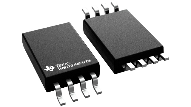
TPS1100PW
ActiveSINGLE P-CHANNEL ENHANCEMENT-MODE MOSFET 8-TSSOP
Deep-Dive with AI
Search across all available documentation for this part.
TPS1100PW
ActiveSINGLE P-CHANNEL ENHANCEMENT-MODE MOSFET 8-TSSOP
Deep-Dive with AI
Technical Specifications
Parameters and characteristics commom to parts in this series
| Specification | TPS1100PW | TPS1100 Series |
|---|---|---|
| Current - Continuous Drain (Id) @ 25°C | 1.27 A | 1.27 - 1.6 A |
| Drain to Source Voltage (Vdss) | 15 V | 15 V |
| Drive Voltage (Max Rds On, Min Rds On) | 10 V, 2.7 V | 2.7 - 10 V |
| FET Type | P-Channel | P-Channel |
| Gate Charge (Qg) (Max) @ Vgs | 5.45 nC | 5.45 nC |
| Mounting Type | Surface Mount | Surface Mount |
| Operating Temperature [Max] | 150 C | 150 C |
| Operating Temperature [Min] | -40 °C | -40 °C |
| Package / Case | 8-TSSOP (0.173", 4.40mm Width) | 8-TSSOP (0.173", 4.40mm Width), 8-SOIC |
| Package / Case | - | 3.9 mm |
| Power Dissipation (Max) [Max] | 504 mW | 504 - 791 mW |
| Rds On (Max) @ Id, Vgs [Max] | 180 mOhm | 180 mOhm |
| Supplier Device Package | 8-TSSOP | 8-TSSOP, 8-SOIC |
| Technology | MOSFET (Metal Oxide) | MOSFET (Metal Oxide) |
| Vgs (Max) | -15 V, 2 V | -15 - 2 V |
| Vgs(th) (Max) @ Id | 1.5 V | 1.5 V |
Pricing
Prices provided here are for design reference only. For realtime values and availability, please visit the distributors directly
TPS1100 Series
Single P-channel Enhancement-Mode MOSFET
| Part | Drain to Source Voltage (Vdss) | Rds On (Max) @ Id, Vgs [Max] | Current - Continuous Drain (Id) @ 25°C | Package / Case | Operating Temperature [Max] | Operating Temperature [Min] | Technology | Drive Voltage (Max Rds On, Min Rds On) | Vgs (Max) | Vgs(th) (Max) @ Id | FET Type | Mounting Type | Power Dissipation (Max) [Max] | Supplier Device Package | Gate Charge (Qg) (Max) @ Vgs | Package / Case |
|---|---|---|---|---|---|---|---|---|---|---|---|---|---|---|---|---|
Texas Instruments TPS1100PWThe TPS1100 is a single P-channel enhancement-mode MOSFET. The device has been optimized for 3-V or 5-V power distribution in battery-powered systems by means of Texas Instruments LinBiCMOSTMprocess. With a maximum VGS(th)of -1.5 V and an IDSSof only 0.5 uA, the TPS1100 is the ideal high-side switch for low-voltage, portable battery-management systems where maximizing battery life is a primary concern. The low rDS(on)and excellent ac characteristics (rise time 10 ns typical) make the TPS1100 the logical choice for low-voltage switching applications such as power switches for pulse-width-modulated (PWM) controllers or motor/bridge drivers.
The ultrathin thin shrink small-outline package or TSSOP (PW) version with its smaller footprint and reduction in height fits in places where other P-channel MOSFETs cannot. The size advantage is especially important where board real estate is at a premium and height restrictions do not allow for a small-outline integrated circuit (SOIC) package.
Such applications include notebook computers, personal digital assistants (PDAs), cellular telephones, and PCMCIA cards. For existing designs, the D-packaged version has a pinout common with other p-channel MOSFETs in SOIC packages.
Caution. This device contains circuits to protect its inputs and outputs against damage due to high static voltages or electrostatic fields. These circuits have been qualified to protect this device against electrostatic discharges (ESD) of up to 2 kV according to MIL-STD-883C, Method 3015; however, it is advised that precautions be taken to avoid application of any voltage higher than maximum-rated voltages to these high-impedance circuits.
The TPS1100 is a single P-channel enhancement-mode MOSFET. The device has been optimized for 3-V or 5-V power distribution in battery-powered systems by means of Texas Instruments LinBiCMOSTMprocess. With a maximum VGS(th)of -1.5 V and an IDSSof only 0.5 uA, the TPS1100 is the ideal high-side switch for low-voltage, portable battery-management systems where maximizing battery life is a primary concern. The low rDS(on)and excellent ac characteristics (rise time 10 ns typical) make the TPS1100 the logical choice for low-voltage switching applications such as power switches for pulse-width-modulated (PWM) controllers or motor/bridge drivers.
The ultrathin thin shrink small-outline package or TSSOP (PW) version with its smaller footprint and reduction in height fits in places where other P-channel MOSFETs cannot. The size advantage is especially important where board real estate is at a premium and height restrictions do not allow for a small-outline integrated circuit (SOIC) package.
Such applications include notebook computers, personal digital assistants (PDAs), cellular telephones, and PCMCIA cards. For existing designs, the D-packaged version has a pinout common with other p-channel MOSFETs in SOIC packages.
Caution. This device contains circuits to protect its inputs and outputs against damage due to high static voltages or electrostatic fields. These circuits have been qualified to protect this device against electrostatic discharges (ESD) of up to 2 kV according to MIL-STD-883C, Method 3015; however, it is advised that precautions be taken to avoid application of any voltage higher than maximum-rated voltages to these high-impedance circuits. | 15 V | 180 mOhm | 1.27 A | 8-TSSOP (0.173", 4.40mm Width) | 150 C | -40 °C | MOSFET (Metal Oxide) | 2.7 V, 10 V | -15 V, 2 V | 1.5 V | P-Channel | Surface Mount | 504 mW | 8-TSSOP | 5.45 nC | |
Texas Instruments TPS1100DThe TPS1100 is a single P-channel enhancement-mode MOSFET. The device has been optimized for 3-V or 5-V power distribution in battery-powered systems by means of Texas Instruments LinBiCMOSTMprocess. With a maximum VGS(th)of -1.5 V and an IDSSof only 0.5 uA, the TPS1100 is the ideal high-side switch for low-voltage, portable battery-management systems where maximizing battery life is a primary concern. The low rDS(on)and excellent ac characteristics (rise time 10 ns typical) make the TPS1100 the logical choice for low-voltage switching applications such as power switches for pulse-width-modulated (PWM) controllers or motor/bridge drivers.
The ultrathin thin shrink small-outline package or TSSOP (PW) version with its smaller footprint and reduction in height fits in places where other P-channel MOSFETs cannot. The size advantage is especially important where board real estate is at a premium and height restrictions do not allow for a small-outline integrated circuit (SOIC) package.
Such applications include notebook computers, personal digital assistants (PDAs), cellular telephones, and PCMCIA cards. For existing designs, the D-packaged version has a pinout common with other p-channel MOSFETs in SOIC packages.
Caution. This device contains circuits to protect its inputs and outputs against damage due to high static voltages or electrostatic fields. These circuits have been qualified to protect this device against electrostatic discharges (ESD) of up to 2 kV according to MIL-STD-883C, Method 3015; however, it is advised that precautions be taken to avoid application of any voltage higher than maximum-rated voltages to these high-impedance circuits.
The TPS1100 is a single P-channel enhancement-mode MOSFET. The device has been optimized for 3-V or 5-V power distribution in battery-powered systems by means of Texas Instruments LinBiCMOSTMprocess. With a maximum VGS(th)of -1.5 V and an IDSSof only 0.5 uA, the TPS1100 is the ideal high-side switch for low-voltage, portable battery-management systems where maximizing battery life is a primary concern. The low rDS(on)and excellent ac characteristics (rise time 10 ns typical) make the TPS1100 the logical choice for low-voltage switching applications such as power switches for pulse-width-modulated (PWM) controllers or motor/bridge drivers.
The ultrathin thin shrink small-outline package or TSSOP (PW) version with its smaller footprint and reduction in height fits in places where other P-channel MOSFETs cannot. The size advantage is especially important where board real estate is at a premium and height restrictions do not allow for a small-outline integrated circuit (SOIC) package.
Such applications include notebook computers, personal digital assistants (PDAs), cellular telephones, and PCMCIA cards. For existing designs, the D-packaged version has a pinout common with other p-channel MOSFETs in SOIC packages.
Caution. This device contains circuits to protect its inputs and outputs against damage due to high static voltages or electrostatic fields. These circuits have been qualified to protect this device against electrostatic discharges (ESD) of up to 2 kV according to MIL-STD-883C, Method 3015; however, it is advised that precautions be taken to avoid application of any voltage higher than maximum-rated voltages to these high-impedance circuits. | 15 V | 180 mOhm | 1.6 A | 8-SOIC | 150 C | -40 °C | MOSFET (Metal Oxide) | 2.7 V, 10 V | -15 V, 2 V | 1.5 V | P-Channel | Surface Mount | 791 mW | 8-SOIC | 5.45 nC | 3.9 mm |
Texas Instruments TPS1100DRThe TPS1100 is a single P-channel enhancement-mode MOSFET. The device has been optimized for 3-V or 5-V power distribution in battery-powered systems by means of Texas Instruments LinBiCMOSTMprocess. With a maximum VGS(th)of -1.5 V and an IDSSof only 0.5 uA, the TPS1100 is the ideal high-side switch for low-voltage, portable battery-management systems where maximizing battery life is a primary concern. The low rDS(on)and excellent ac characteristics (rise time 10 ns typical) make the TPS1100 the logical choice for low-voltage switching applications such as power switches for pulse-width-modulated (PWM) controllers or motor/bridge drivers.
The ultrathin thin shrink small-outline package or TSSOP (PW) version with its smaller footprint and reduction in height fits in places where other P-channel MOSFETs cannot. The size advantage is especially important where board real estate is at a premium and height restrictions do not allow for a small-outline integrated circuit (SOIC) package.
Such applications include notebook computers, personal digital assistants (PDAs), cellular telephones, and PCMCIA cards. For existing designs, the D-packaged version has a pinout common with other p-channel MOSFETs in SOIC packages.
Caution. This device contains circuits to protect its inputs and outputs against damage due to high static voltages or electrostatic fields. These circuits have been qualified to protect this device against electrostatic discharges (ESD) of up to 2 kV according to MIL-STD-883C, Method 3015; however, it is advised that precautions be taken to avoid application of any voltage higher than maximum-rated voltages to these high-impedance circuits.
The TPS1100 is a single P-channel enhancement-mode MOSFET. The device has been optimized for 3-V or 5-V power distribution in battery-powered systems by means of Texas Instruments LinBiCMOSTMprocess. With a maximum VGS(th)of -1.5 V and an IDSSof only 0.5 uA, the TPS1100 is the ideal high-side switch for low-voltage, portable battery-management systems where maximizing battery life is a primary concern. The low rDS(on)and excellent ac characteristics (rise time 10 ns typical) make the TPS1100 the logical choice for low-voltage switching applications such as power switches for pulse-width-modulated (PWM) controllers or motor/bridge drivers.
The ultrathin thin shrink small-outline package or TSSOP (PW) version with its smaller footprint and reduction in height fits in places where other P-channel MOSFETs cannot. The size advantage is especially important where board real estate is at a premium and height restrictions do not allow for a small-outline integrated circuit (SOIC) package.
Such applications include notebook computers, personal digital assistants (PDAs), cellular telephones, and PCMCIA cards. For existing designs, the D-packaged version has a pinout common with other p-channel MOSFETs in SOIC packages.
Caution. This device contains circuits to protect its inputs and outputs against damage due to high static voltages or electrostatic fields. These circuits have been qualified to protect this device against electrostatic discharges (ESD) of up to 2 kV according to MIL-STD-883C, Method 3015; however, it is advised that precautions be taken to avoid application of any voltage higher than maximum-rated voltages to these high-impedance circuits. | 15 V | 180 mOhm | 1.6 A | 8-SOIC | 150 C | -40 °C | MOSFET (Metal Oxide) | 2.7 V, 10 V | -15 V, 2 V | 1.5 V | P-Channel | Surface Mount | 791 mW | 8-SOIC | 5.45 nC | 3.9 mm |
Texas Instruments TPS1100PWRThe TPS1100 is a single P-channel enhancement-mode MOSFET. The device has been optimized for 3-V or 5-V power distribution in battery-powered systems by means of Texas Instruments LinBiCMOSTMprocess. With a maximum VGS(th)of -1.5 V and an IDSSof only 0.5 uA, the TPS1100 is the ideal high-side switch for low-voltage, portable battery-management systems where maximizing battery life is a primary concern. The low rDS(on)and excellent ac characteristics (rise time 10 ns typical) make the TPS1100 the logical choice for low-voltage switching applications such as power switches for pulse-width-modulated (PWM) controllers or motor/bridge drivers.
The ultrathin thin shrink small-outline package or TSSOP (PW) version with its smaller footprint and reduction in height fits in places where other P-channel MOSFETs cannot. The size advantage is especially important where board real estate is at a premium and height restrictions do not allow for a small-outline integrated circuit (SOIC) package.
Such applications include notebook computers, personal digital assistants (PDAs), cellular telephones, and PCMCIA cards. For existing designs, the D-packaged version has a pinout common with other p-channel MOSFETs in SOIC packages.
Caution. This device contains circuits to protect its inputs and outputs against damage due to high static voltages or electrostatic fields. These circuits have been qualified to protect this device against electrostatic discharges (ESD) of up to 2 kV according to MIL-STD-883C, Method 3015; however, it is advised that precautions be taken to avoid application of any voltage higher than maximum-rated voltages to these high-impedance circuits.
The TPS1100 is a single P-channel enhancement-mode MOSFET. The device has been optimized for 3-V or 5-V power distribution in battery-powered systems by means of Texas Instruments LinBiCMOSTMprocess. With a maximum VGS(th)of -1.5 V and an IDSSof only 0.5 uA, the TPS1100 is the ideal high-side switch for low-voltage, portable battery-management systems where maximizing battery life is a primary concern. The low rDS(on)and excellent ac characteristics (rise time 10 ns typical) make the TPS1100 the logical choice for low-voltage switching applications such as power switches for pulse-width-modulated (PWM) controllers or motor/bridge drivers.
The ultrathin thin shrink small-outline package or TSSOP (PW) version with its smaller footprint and reduction in height fits in places where other P-channel MOSFETs cannot. The size advantage is especially important where board real estate is at a premium and height restrictions do not allow for a small-outline integrated circuit (SOIC) package.
Such applications include notebook computers, personal digital assistants (PDAs), cellular telephones, and PCMCIA cards. For existing designs, the D-packaged version has a pinout common with other p-channel MOSFETs in SOIC packages.
Caution. This device contains circuits to protect its inputs and outputs against damage due to high static voltages or electrostatic fields. These circuits have been qualified to protect this device against electrostatic discharges (ESD) of up to 2 kV according to MIL-STD-883C, Method 3015; however, it is advised that precautions be taken to avoid application of any voltage higher than maximum-rated voltages to these high-impedance circuits. | 15 V | 180 mOhm | 1.27 A | 8-TSSOP (0.173", 4.40mm Width) | 150 C | -40 °C | MOSFET (Metal Oxide) | 2.7 V, 10 V | -15 V, 2 V | 1.5 V | P-Channel | Surface Mount | 504 mW | 8-TSSOP | 5.45 nC |
Description
General part information
TPS1100 Series
The TPS1100 is a single P-channel enhancement-mode MOSFET. The device has been optimized for 3-V or 5-V power distribution in battery-powered systems by means of Texas Instruments LinBiCMOSTMprocess. With a maximum VGS(th)of -1.5 V and an IDSSof only 0.5 uA, the TPS1100 is the ideal high-side switch for low-voltage, portable battery-management systems where maximizing battery life is a primary concern. The low rDS(on)and excellent ac characteristics (rise time 10 ns typical) make the TPS1100 the logical choice for low-voltage switching applications such as power switches for pulse-width-modulated (PWM) controllers or motor/bridge drivers.
The ultrathin thin shrink small-outline package or TSSOP (PW) version with its smaller footprint and reduction in height fits in places where other P-channel MOSFETs cannot. The size advantage is especially important where board real estate is at a premium and height restrictions do not allow for a small-outline integrated circuit (SOIC) package.
Such applications include notebook computers, personal digital assistants (PDAs), cellular telephones, and PCMCIA cards. For existing designs, the D-packaged version has a pinout common with other p-channel MOSFETs in SOIC packages.
Documents
Technical documentation and resources