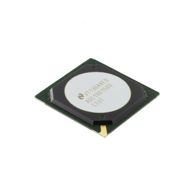
ADC12D1600RFIUT/NOPB
Active12-BIT, DUAL 1.6-GSPS OR SINGLE 3.2-GSPS, RF-SAMPLING ANALOG-TO-DIGITAL CONVERTER (ADC)
Deep-Dive with AI
Search across all available documentation for this part.
ADC12D1600RFIUT/NOPB
Active12-BIT, DUAL 1.6-GSPS OR SINGLE 3.2-GSPS, RF-SAMPLING ANALOG-TO-DIGITAL CONVERTER (ADC)
Technical Specifications
Parameters and characteristics commom to parts in this series
| Specification | ADC12D1600RFIUT/NOPB | ADC12D1600 Series |
|---|---|---|
| Architecture | Folding Interpolating | Folding Interpolating |
| Configuration | MUX-S/H-ADC | MUX-S/H-ADC |
| Data Interface | LVDS - Parallel | LVDS - Parallel |
| Features | Simultaneous Sampling | Simultaneous Sampling |
| Input Type | Differential | Differential |
| Mounting Type | Surface Mount | Surface Mount |
| Number of A/D Converters | 2 | 2 |
| Number of Bits | 12 | 12 |
| Number of Inputs | 2 | 2 |
| Operating Temperature [Max] | 85 °C | 85 °C |
| Operating Temperature [Min] | -40 °C | -40 °C |
| Package / Case | 292-BBGA | 292-BBGA |
| Ratio - S/H:ADC | 1:1 | 1:1 |
| Reference Type | Internal | Internal |
| Sampling Rate (Per Second) | 3.2 G | 3.2 G |
| Supplier Device Package | 292-BGA | 292-BGA |
| Voltage - Supply, Analog [Max] | 2 V | 2 V |
| Voltage - Supply, Analog [Min] | 1.8 V | 1.8 V |
| Voltage - Supply, Digital [Max] | 2 V | 2 V |
| Voltage - Supply, Digital [Min] | 1.8 V | 1.8 V |
Pricing
Prices provided here are for design reference only. For realtime values and availability, please visit the distributors directly
ADC12D1600 Series
12-bit, dual 1.6-GSPS or single 3.2-GSPS analog-to-digital converter (ADC)
| Part | Ratio - S/H:ADC | Mounting Type | Number of A/D Converters | Architecture | Configuration | Voltage - Supply, Digital [Min] | Voltage - Supply, Digital [Max] | Number of Inputs | Data Interface | Input Type | Number of Bits | Voltage - Supply, Analog [Min] | Voltage - Supply, Analog [Max] | Reference Type | Package / Case | Supplier Device Package | Sampling Rate (Per Second) | Features | Operating Temperature [Min] | Operating Temperature [Max] |
|---|---|---|---|---|---|---|---|---|---|---|---|---|---|---|---|---|---|---|---|---|
Texas Instruments ADC12D1600CIUTThe 12-bit, 2.0/3.2 GSPS ADC12D1x00 device is the latest advance in TI’s Ultra High-Speed ADC family and builds upon the features, architecture, and functionality of the 10-bit GHz family of ADCs.
The ADC12D1x00 provides a flexible LVDS interface which has multiple SPI programmable options to facilitate board design and FPGA/ASIC data capture. The LVDS outputs are compatible with IEEE 1596.3-1996 and support programmable common-mode voltage.
The ADC12D1x00 is packaged in a leaded or lead-free 292-pin thermally enhanced BGA package over the rated industrial temperature range of –40°C to 85°C.
The 12-bit, 2.0/3.2 GSPS ADC12D1x00 device is the latest advance in TI’s Ultra High-Speed ADC family and builds upon the features, architecture, and functionality of the 10-bit GHz family of ADCs.
The ADC12D1x00 provides a flexible LVDS interface which has multiple SPI programmable options to facilitate board design and FPGA/ASIC data capture. The LVDS outputs are compatible with IEEE 1596.3-1996 and support programmable common-mode voltage.
The ADC12D1x00 is packaged in a leaded or lead-free 292-pin thermally enhanced BGA package over the rated industrial temperature range of –40°C to 85°C. | 1:1 | Surface Mount | 2 | Folding Interpolating | MUX-S/H-ADC | 1.8 V | 2 V | 2 | LVDS - Parallel | Differential | 12 | 1.8 V | 2 V | Internal | 292-BBGA | 292-BGA | 3.2 G | Simultaneous Sampling | -40 °C | 85 °C |
Texas Instruments ADC12D1600RFIUT/NOPBThe 12-bit 3.2- and 2-GSPS ADC12D1x00RF is an RF-sampling GSPS ADC that can directly sample input frequencies up to and above 2.7 GHz. The ADC12D1x00RF augments the very large Nyquist zone of TI’s GSPS ADCs with excellent noise and linearity performance at RF frequencies, extending its usable range beyond the 3rdNyquist zone
The ADC12D1x00RF provides a flexible LVDS interface which has multiple SPI programmable options to facilitate board design and FPGA/ASIC data capture. The LVDS outputs are compatible with IEEE 1596.3-1996 and supports programmable common-mode voltage. The product is packaged in a lead-free 292-ball thermally enhanced BGA package over the rated industrial temperature range of –40°C to 85°C.
The 12-bit 3.2- and 2-GSPS ADC12D1x00RF is an RF-sampling GSPS ADC that can directly sample input frequencies up to and above 2.7 GHz. The ADC12D1x00RF augments the very large Nyquist zone of TI’s GSPS ADCs with excellent noise and linearity performance at RF frequencies, extending its usable range beyond the 3rdNyquist zone
The ADC12D1x00RF provides a flexible LVDS interface which has multiple SPI programmable options to facilitate board design and FPGA/ASIC data capture. The LVDS outputs are compatible with IEEE 1596.3-1996 and supports programmable common-mode voltage. The product is packaged in a lead-free 292-ball thermally enhanced BGA package over the rated industrial temperature range of –40°C to 85°C. | 1:1 | Surface Mount | 2 | Folding Interpolating | MUX-S/H-ADC | 1.8 V | 2 V | 2 | LVDS - Parallel | Differential | 12 | 1.8 V | 2 V | Internal | 292-BBGA | 292-BGA | 3.2 G | Simultaneous Sampling | -40 °C | 85 °C |
Texas Instruments ADC12D1600RFIUTThe 12-bit 3.2- and 2-GSPS ADC12D1x00RF is an RF-sampling GSPS ADC that can directly sample input frequencies up to and above 2.7 GHz. The ADC12D1x00RF augments the very large Nyquist zone of TI’s GSPS ADCs with excellent noise and linearity performance at RF frequencies, extending its usable range beyond the 3rdNyquist zone
The ADC12D1x00RF provides a flexible LVDS interface which has multiple SPI programmable options to facilitate board design and FPGA/ASIC data capture. The LVDS outputs are compatible with IEEE 1596.3-1996 and supports programmable common-mode voltage. The product is packaged in a lead-free 292-ball thermally enhanced BGA package over the rated industrial temperature range of –40°C to 85°C.
The 12-bit 3.2- and 2-GSPS ADC12D1x00RF is an RF-sampling GSPS ADC that can directly sample input frequencies up to and above 2.7 GHz. The ADC12D1x00RF augments the very large Nyquist zone of TI’s GSPS ADCs with excellent noise and linearity performance at RF frequencies, extending its usable range beyond the 3rdNyquist zone
The ADC12D1x00RF provides a flexible LVDS interface which has multiple SPI programmable options to facilitate board design and FPGA/ASIC data capture. The LVDS outputs are compatible with IEEE 1596.3-1996 and supports programmable common-mode voltage. The product is packaged in a lead-free 292-ball thermally enhanced BGA package over the rated industrial temperature range of –40°C to 85°C. | 1:1 | Surface Mount | 2 | Folding Interpolating | MUX-S/H-ADC | 1.8 V | 2 V | 2 | LVDS - Parallel | Differential | 12 | 1.8 V | 2 V | Internal | 292-BBGA | 292-BGA | 3.2 G | Simultaneous Sampling | -40 °C | 85 °C |
Texas Instruments ADC12D1600CIUT/NOPBThe 12-bit, 2.0/3.2 GSPS ADC12D1x00 device is the latest advance in TI’s Ultra High-Speed ADC family and builds upon the features, architecture, and functionality of the 10-bit GHz family of ADCs.
The ADC12D1x00 provides a flexible LVDS interface which has multiple SPI programmable options to facilitate board design and FPGA/ASIC data capture. The LVDS outputs are compatible with IEEE 1596.3-1996 and support programmable common-mode voltage.
The ADC12D1x00 is packaged in a leaded or lead-free 292-pin thermally enhanced BGA package over the rated industrial temperature range of –40°C to 85°C.
The 12-bit, 2.0/3.2 GSPS ADC12D1x00 device is the latest advance in TI’s Ultra High-Speed ADC family and builds upon the features, architecture, and functionality of the 10-bit GHz family of ADCs.
The ADC12D1x00 provides a flexible LVDS interface which has multiple SPI programmable options to facilitate board design and FPGA/ASIC data capture. The LVDS outputs are compatible with IEEE 1596.3-1996 and support programmable common-mode voltage.
The ADC12D1x00 is packaged in a leaded or lead-free 292-pin thermally enhanced BGA package over the rated industrial temperature range of –40°C to 85°C. | Surface Mount | 2 | 12 | 292-BBGA | 292-BGA | 3.2 G | -40 °C | 85 °C |
Description
General part information
ADC12D1600 Series
The 12-bit, 2.0/3.2 GSPS ADC12D1x00 device is the latest advance in TI’s Ultra High-Speed ADC family and builds upon the features, architecture, and functionality of the 10-bit GHz family of ADCs.
The ADC12D1x00 provides a flexible LVDS interface which has multiple SPI programmable options to facilitate board design and FPGA/ASIC data capture. The LVDS outputs are compatible with IEEE 1596.3-1996 and support programmable common-mode voltage.
The ADC12D1x00 is packaged in a leaded or lead-free 292-pin thermally enhanced BGA package over the rated industrial temperature range of –40°C to 85°C.
Documents
Technical documentation and resources