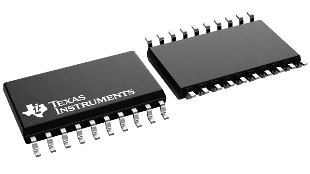
TPIC6595DW
Active8-BIT SHIFT REGISTER WITH 250MA/CH 20-SOIC -40 TO 125
Deep-Dive with AI
Search across all available documentation for this part.
TPIC6595DW
Active8-BIT SHIFT REGISTER WITH 250MA/CH 20-SOIC -40 TO 125
Technical Specifications
Parameters and characteristics commom to parts in this series
| Specification | TPIC6595DW | TPIC6595 Series |
|---|---|---|
| Function | Serial to Parallel, Serial | Serial to Parallel, Serial |
| Logic Type | Shift Register | Shift Register |
| Mounting Type | Surface Mount | Surface Mount, Through Hole |
| Number of Bits per Element | 8 | 8 |
| Number of Elements [custom] | 1 | 1 |
| Operating Temperature [Max] | 125 °C | 125 °C |
| Operating Temperature [Min] | -40 °C | -40 °C |
| Output Type | Open Drain | Open Drain |
| Package / Case | 7.5 mm, 0.295 in | 0.295 - 7.5 mm |
| Package / Case | 20-SOIC | 20-SOIC, 20-DIP |
| Package / Case | - | 0.3 in |
| Package / Case | - | 7.62 mm |
| Supplier Device Package | 20-SOIC | 20-SOIC, 20-PDIP |
| Voltage - Supply [Max] | 5.5 V | 5.5 V |
| Voltage - Supply [Min] | 4.5 V | 4.5 V |
Pricing
Prices provided here are for design reference only. For realtime values and availability, please visit the distributors directly
TPIC6595 Series
8-bit shift register with 250mA/ch
| Part | Supplier Device Package | Logic Type | Voltage - Supply [Max] | Voltage - Supply [Min] | Number of Elements [custom] | Package / Case | Package / Case | Operating Temperature [Max] | Operating Temperature [Min] | Mounting Type | Function | Output Type | Number of Bits per Element | Package / Case | Package / Case |
|---|---|---|---|---|---|---|---|---|---|---|---|---|---|---|---|
Texas Instruments TPIC6595DWG4The TPIC6595 is a monolithic, high-voltage, high-current power 8-bit shift register designed for use in systems that require relatively high load power. The device contains a built-in voltage clamp on the outputs for inductive transient protection. Power driver applications include relays, solenoids, and other medium-current or high-voltage loads.
This device contains an 8-bit serial-in, parallel-out shift register that feeds an 8-bit D-type storage register. Data transfers through both the shift and storage registers on the rising edge of the shift-register clock (SRCK) and the register clock (RCK) respectively. The storage register transfers data to the output buffer when shift register clear (SRCLR) is high. Write data and read data are valid only when RCK is low. When SRCLR is low, the input shift register is cleared. When output enable (G) is held high, all data in the output buffers is held low and all drain outputs are off. When G is held low, data from the storage register is transparent to the output buffers. The serial output (SER OUT) allows for cascading of the data from the shift register to additional devices.
Outputs are low-side, open-drain DMOS transistors with output ratings of 45V and 250mA continuous sink current capability. When data in the output buffers is low, the DMOS-transistor outputs are off. When data is high, the DMOS-transistor outputs have sink current capability.
Separate power and logic level ground pins are provided to facilitate maximum system flexibility. Pins 1, 10, 11, and 20 are internally connected, and each pin must be externally connected to the power system ground in order to minimize parasitic inductance. A single-point connection between pin 19, logic ground (LGND), and pins 1, 10, 11, and 20, power grounds (PGND), must be externally made in a manner that reduces crosstalk between the logic and load circuits. The TPIC6595 is characterized for operation over the operating case temperature range of −40°C to 125°C.
The TPIC6595 is a monolithic, high-voltage, high-current power 8-bit shift register designed for use in systems that require relatively high load power. The device contains a built-in voltage clamp on the outputs for inductive transient protection. Power driver applications include relays, solenoids, and other medium-current or high-voltage loads.
This device contains an 8-bit serial-in, parallel-out shift register that feeds an 8-bit D-type storage register. Data transfers through both the shift and storage registers on the rising edge of the shift-register clock (SRCK) and the register clock (RCK) respectively. The storage register transfers data to the output buffer when shift register clear (SRCLR) is high. Write data and read data are valid only when RCK is low. When SRCLR is low, the input shift register is cleared. When output enable (G) is held high, all data in the output buffers is held low and all drain outputs are off. When G is held low, data from the storage register is transparent to the output buffers. The serial output (SER OUT) allows for cascading of the data from the shift register to additional devices.
Outputs are low-side, open-drain DMOS transistors with output ratings of 45V and 250mA continuous sink current capability. When data in the output buffers is low, the DMOS-transistor outputs are off. When data is high, the DMOS-transistor outputs have sink current capability.
Separate power and logic level ground pins are provided to facilitate maximum system flexibility. Pins 1, 10, 11, and 20 are internally connected, and each pin must be externally connected to the power system ground in order to minimize parasitic inductance. A single-point connection between pin 19, logic ground (LGND), and pins 1, 10, 11, and 20, power grounds (PGND), must be externally made in a manner that reduces crosstalk between the logic and load circuits. The TPIC6595 is characterized for operation over the operating case temperature range of −40°C to 125°C. | 20-SOIC | Shift Register | 5.5 V | 4.5 V | 1 | 0.295 in, 7.5 mm | 20-SOIC | 125 °C | -40 °C | Surface Mount | Serial to Parallel, Serial | Open Drain | 8 | ||
Texas Instruments TPIC6595NThe TPIC6595 is a monolithic, high-voltage, high-current power 8-bit shift register designed for use in systems that require relatively high load power. The device contains a built-in voltage clamp on the outputs for inductive transient protection. Power driver applications include relays, solenoids, and other medium-current or high-voltage loads.
This device contains an 8-bit serial-in, parallel-out shift register that feeds an 8-bit D-type storage register. Data transfers through both the shift and storage registers on the rising edge of the shift-register clock (SRCK) and the register clock (RCK) respectively. The storage register transfers data to the output buffer when shift register clear (SRCLR) is high. Write data and read data are valid only when RCK is low. When SRCLR is low, the input shift register is cleared. When output enable (G) is held high, all data in the output buffers is held low and all drain outputs are off. When G is held low, data from the storage register is transparent to the output buffers. The serial output (SER OUT) allows for cascading of the data from the shift register to additional devices.
Outputs are low-side, open-drain DMOS transistors with output ratings of 45V and 250mA continuous sink current capability. When data in the output buffers is low, the DMOS-transistor outputs are off. When data is high, the DMOS-transistor outputs have sink current capability.
Separate power and logic level ground pins are provided to facilitate maximum system flexibility. Pins 1, 10, 11, and 20 are internally connected, and each pin must be externally connected to the power system ground in order to minimize parasitic inductance. A single-point connection between pin 19, logic ground (LGND), and pins 1, 10, 11, and 20, power grounds (PGND), must be externally made in a manner that reduces crosstalk between the logic and load circuits. The TPIC6595 is characterized for operation over the operating case temperature range of −40°C to 125°C.
The TPIC6595 is a monolithic, high-voltage, high-current power 8-bit shift register designed for use in systems that require relatively high load power. The device contains a built-in voltage clamp on the outputs for inductive transient protection. Power driver applications include relays, solenoids, and other medium-current or high-voltage loads.
This device contains an 8-bit serial-in, parallel-out shift register that feeds an 8-bit D-type storage register. Data transfers through both the shift and storage registers on the rising edge of the shift-register clock (SRCK) and the register clock (RCK) respectively. The storage register transfers data to the output buffer when shift register clear (SRCLR) is high. Write data and read data are valid only when RCK is low. When SRCLR is low, the input shift register is cleared. When output enable (G) is held high, all data in the output buffers is held low and all drain outputs are off. When G is held low, data from the storage register is transparent to the output buffers. The serial output (SER OUT) allows for cascading of the data from the shift register to additional devices.
Outputs are low-side, open-drain DMOS transistors with output ratings of 45V and 250mA continuous sink current capability. When data in the output buffers is low, the DMOS-transistor outputs are off. When data is high, the DMOS-transistor outputs have sink current capability.
Separate power and logic level ground pins are provided to facilitate maximum system flexibility. Pins 1, 10, 11, and 20 are internally connected, and each pin must be externally connected to the power system ground in order to minimize parasitic inductance. A single-point connection between pin 19, logic ground (LGND), and pins 1, 10, 11, and 20, power grounds (PGND), must be externally made in a manner that reduces crosstalk between the logic and load circuits. The TPIC6595 is characterized for operation over the operating case temperature range of −40°C to 125°C. | 20-PDIP | Shift Register | 5.5 V | 4.5 V | 1 | 20-DIP | 125 °C | -40 °C | Through Hole | Serial to Parallel, Serial | Open Drain | 8 | 0.3 in | 7.62 mm | |
Texas Instruments TPIC6595DWRG4The TPIC6595 is a monolithic, high-voltage, high-current power 8-bit shift register designed for use in systems that require relatively high load power. The device contains a built-in voltage clamp on the outputs for inductive transient protection. Power driver applications include relays, solenoids, and other medium-current or high-voltage loads.
This device contains an 8-bit serial-in, parallel-out shift register that feeds an 8-bit D-type storage register. Data transfers through both the shift and storage registers on the rising edge of the shift-register clock (SRCK) and the register clock (RCK) respectively. The storage register transfers data to the output buffer when shift register clear (SRCLR) is high. Write data and read data are valid only when RCK is low. When SRCLR is low, the input shift register is cleared. When output enable (G) is held high, all data in the output buffers is held low and all drain outputs are off. When G is held low, data from the storage register is transparent to the output buffers. The serial output (SER OUT) allows for cascading of the data from the shift register to additional devices.
Outputs are low-side, open-drain DMOS transistors with output ratings of 45V and 250mA continuous sink current capability. When data in the output buffers is low, the DMOS-transistor outputs are off. When data is high, the DMOS-transistor outputs have sink current capability.
Separate power and logic level ground pins are provided to facilitate maximum system flexibility. Pins 1, 10, 11, and 20 are internally connected, and each pin must be externally connected to the power system ground in order to minimize parasitic inductance. A single-point connection between pin 19, logic ground (LGND), and pins 1, 10, 11, and 20, power grounds (PGND), must be externally made in a manner that reduces crosstalk between the logic and load circuits. The TPIC6595 is characterized for operation over the operating case temperature range of −40°C to 125°C.
The TPIC6595 is a monolithic, high-voltage, high-current power 8-bit shift register designed for use in systems that require relatively high load power. The device contains a built-in voltage clamp on the outputs for inductive transient protection. Power driver applications include relays, solenoids, and other medium-current or high-voltage loads.
This device contains an 8-bit serial-in, parallel-out shift register that feeds an 8-bit D-type storage register. Data transfers through both the shift and storage registers on the rising edge of the shift-register clock (SRCK) and the register clock (RCK) respectively. The storage register transfers data to the output buffer when shift register clear (SRCLR) is high. Write data and read data are valid only when RCK is low. When SRCLR is low, the input shift register is cleared. When output enable (G) is held high, all data in the output buffers is held low and all drain outputs are off. When G is held low, data from the storage register is transparent to the output buffers. The serial output (SER OUT) allows for cascading of the data from the shift register to additional devices.
Outputs are low-side, open-drain DMOS transistors with output ratings of 45V and 250mA continuous sink current capability. When data in the output buffers is low, the DMOS-transistor outputs are off. When data is high, the DMOS-transistor outputs have sink current capability.
Separate power and logic level ground pins are provided to facilitate maximum system flexibility. Pins 1, 10, 11, and 20 are internally connected, and each pin must be externally connected to the power system ground in order to minimize parasitic inductance. A single-point connection between pin 19, logic ground (LGND), and pins 1, 10, 11, and 20, power grounds (PGND), must be externally made in a manner that reduces crosstalk between the logic and load circuits. The TPIC6595 is characterized for operation over the operating case temperature range of −40°C to 125°C. | 20-SOIC | Shift Register | 5.5 V | 4.5 V | 1 | 0.295 in, 7.5 mm | 20-SOIC | 125 °C | -40 °C | Surface Mount | Serial to Parallel, Serial | Open Drain | 8 | ||
Texas Instruments TPIC6595DWThe TPIC6595 is a monolithic, high-voltage, high-current power 8-bit shift register designed for use in systems that require relatively high load power. The device contains a built-in voltage clamp on the outputs for inductive transient protection. Power driver applications include relays, solenoids, and other medium-current or high-voltage loads.
This device contains an 8-bit serial-in, parallel-out shift register that feeds an 8-bit D-type storage register. Data transfers through both the shift and storage registers on the rising edge of the shift-register clock (SRCK) and the register clock (RCK) respectively. The storage register transfers data to the output buffer when shift register clear (SRCLR) is high. Write data and read data are valid only when RCK is low. When SRCLR is low, the input shift register is cleared. When output enable (G) is held high, all data in the output buffers is held low and all drain outputs are off. When G is held low, data from the storage register is transparent to the output buffers. The serial output (SER OUT) allows for cascading of the data from the shift register to additional devices.
Outputs are low-side, open-drain DMOS transistors with output ratings of 45V and 250mA continuous sink current capability. When data in the output buffers is low, the DMOS-transistor outputs are off. When data is high, the DMOS-transistor outputs have sink current capability.
Separate power and logic level ground pins are provided to facilitate maximum system flexibility. Pins 1, 10, 11, and 20 are internally connected, and each pin must be externally connected to the power system ground in order to minimize parasitic inductance. A single-point connection between pin 19, logic ground (LGND), and pins 1, 10, 11, and 20, power grounds (PGND), must be externally made in a manner that reduces crosstalk between the logic and load circuits. The TPIC6595 is characterized for operation over the operating case temperature range of −40°C to 125°C.
The TPIC6595 is a monolithic, high-voltage, high-current power 8-bit shift register designed for use in systems that require relatively high load power. The device contains a built-in voltage clamp on the outputs for inductive transient protection. Power driver applications include relays, solenoids, and other medium-current or high-voltage loads.
This device contains an 8-bit serial-in, parallel-out shift register that feeds an 8-bit D-type storage register. Data transfers through both the shift and storage registers on the rising edge of the shift-register clock (SRCK) and the register clock (RCK) respectively. The storage register transfers data to the output buffer when shift register clear (SRCLR) is high. Write data and read data are valid only when RCK is low. When SRCLR is low, the input shift register is cleared. When output enable (G) is held high, all data in the output buffers is held low and all drain outputs are off. When G is held low, data from the storage register is transparent to the output buffers. The serial output (SER OUT) allows for cascading of the data from the shift register to additional devices.
Outputs are low-side, open-drain DMOS transistors with output ratings of 45V and 250mA continuous sink current capability. When data in the output buffers is low, the DMOS-transistor outputs are off. When data is high, the DMOS-transistor outputs have sink current capability.
Separate power and logic level ground pins are provided to facilitate maximum system flexibility. Pins 1, 10, 11, and 20 are internally connected, and each pin must be externally connected to the power system ground in order to minimize parasitic inductance. A single-point connection between pin 19, logic ground (LGND), and pins 1, 10, 11, and 20, power grounds (PGND), must be externally made in a manner that reduces crosstalk between the logic and load circuits. The TPIC6595 is characterized for operation over the operating case temperature range of −40°C to 125°C. | 20-SOIC | Shift Register | 5.5 V | 4.5 V | 1 | 0.295 in, 7.5 mm | 20-SOIC | 125 °C | -40 °C | Surface Mount | Serial to Parallel, Serial | Open Drain | 8 |
Description
General part information
TPIC6595 Series
The TPIC6595 is a monolithic, high-voltage, high-current power 8-bit shift register designed for use in systems that require relatively high load power. The device contains a built-in voltage clamp on the outputs for inductive transient protection. Power driver applications include relays, solenoids, and other medium-current or high-voltage loads.
This device contains an 8-bit serial-in, parallel-out shift register that feeds an 8-bit D-type storage register. Data transfers through both the shift and storage registers on the rising edge of the shift-register clock (SRCK) and the register clock (RCK) respectively. The storage register transfers data to the output buffer when shift register clear (SRCLR) is high. Write data and read data are valid only when RCK is low. When SRCLR is low, the input shift register is cleared. When output enable (G) is held high, all data in the output buffers is held low and all drain outputs are off. When G is held low, data from the storage register is transparent to the output buffers. The serial output (SER OUT) allows for cascading of the data from the shift register to additional devices.
Outputs are low-side, open-drain DMOS transistors with output ratings of 45V and 250mA continuous sink current capability. When data in the output buffers is low, the DMOS-transistor outputs are off. When data is high, the DMOS-transistor outputs have sink current capability.