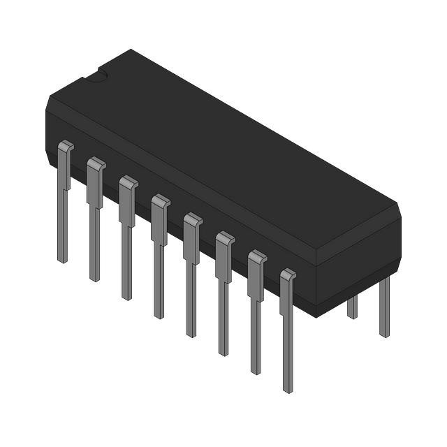
JM38510/66304BEA
ActiveSYNCHRONOUS 4-BIT BINARY COUNTERS 16-CDIP -55 TO 125
Deep-Dive with AI
Search across all available documentation for this part.
JM38510/66304BEA
ActiveSYNCHRONOUS 4-BIT BINARY COUNTERS 16-CDIP -55 TO 125
Deep-Dive with AI
Technical Specifications
Parameters and characteristics commom to parts in this series
| Specification | JM38510/66304BEA | JM38510 Series |
|---|---|---|
| - | - | |
| Amplifier Type | - | J-FET |
| Circuit | - | 1 x 3:8, 8:8 |
| Circuit | - | 4 |
| Circuit | - | 2:1 |
| Clock Frequency | - | 25 - 150 MHz |
| Count Rate | 36 MHz | 11 - 44 MHz |
| Current - Input Bias | - | 50 pA |
| Current - Output High, Low | - | 2 - 300 µA |
| Current - Output High, Low | - | 1 - 400 µA |
| Current - Output High, Low | - | 4 - 60 mA |
| Current - Quiescent (Iq) | - | 4 - 86 mA |
| Current - Quiescent (Max) | - | 5.4 - 44 mA |
| Current - Supply | - | 4 mA |
| Delay Time - Propagation | - | 20 - 28 ns |
| Direction | Up | Up, Down |
| Function | - | Reset, Set(Preset), Universal, Standard |
| Gain Bandwidth Product | - | 3 MHz |
| Grade | - | Military |
| Independent Circuits | - | 1 |
| Input Capacitance | - | 3 pF |
| Input Logic Level - Low | - | 0.7 - 0.8 V |
| Logic Type | Binary Counter | Binary Counter, Peripheral Driver, Register, Bidirectional, NAND Gate, OR Gate, Decade, Counter, INVERT Gate, AND, OR, Parity Generator/Checker, D-Type Transparent Latch, NOR Gate, Inverter, Shift Register, Divide-by-N, Binary Full Adder with Fast Carry |
| Max Propagation Delay @ V, Max CL | - | 5 - 40 ns |
| Max Propagation Delay @ V, Max CL | - | 45 pF |
| Mounting Type | Through Hole | Through Hole, Surface Mount |
| Number of Bits | - | 4 |
| Number of Bits per Element | 4 | 1 - 14 |
| Number of Circuits | - | 1 - 6 |
| Number of Elements [custom] | 1 | 1 - 2 |
| Number of Inputs | - | 2 - 8 |
| Operating Temperature [Max] | 125 °C | 125 °C |
| Operating Temperature [Min] | -55 C | -55 C |
| Output Type | - | Open Collector, Complementary, Non-Inverted, 3-State, Push-Pull, Single-Ended, Tri-State, Non-Inverted |
| Package / Case | 16-CDIP (0.300", 7.62mm) | 16-CDIP (0.300", 7.62mm), 8-CDIP, 14-CDIP, 16-CFlatPack, 20-CLCC, 14-CFlatpack, 20-CFlatPack |
| Package / Case | - | 7.62 mm |
| Package / Case | - | 0.3 in |
| Package / Case | - | 0.3 - 7.62 in |
| Qualification | - | MIL-PRF-38535L |
| Reset | Synchronous | Asynchronous, Synchronous |
| Schmitt Trigger Input | - | False |
| Slew Rate | - | 7 V/µs |
| Supplier Device Package | 16-CDIP | 16-CDIP, 8-CDIP, 14-CDIP, 20-LCCC, 20-CFP |
| Supplier Device Package | - | 8.89 |
| Supplier Device Package | - | 8.89 |
| Supply Voltage | - | 4.5 V |
| Supply Voltage | - | 5.5 V |
| Timing | Synchronous | Synchronous |
| Trigger Type | Positive Edge | Positive Edge, Negative Edge |
| Type | - | JK Type, D-Type, Decoder/Demultiplexer, Data Selector/Multiplexer |
| Voltage - Supply [Max] | 6 V | 5 - 18 V |
| Voltage - Supply [Min] | 2 V | 2 - 4.75 V |
| Voltage Supply Source | - | Single Supply |
Pricing
Prices provided here are for design reference only. For realtime values and availability, please visit the distributors directly
JM38510 Series
AND-OR-INVERT GATE, 4-INPUT, TTL
| Part | Reset | Count Rate | Logic Type | Mounting Type | Operating Temperature [Min] | Operating Temperature [Max] | Supplier Device Package | Voltage - Supply [Max] | Voltage - Supply [Min] | Package / Case | Number of Elements [custom] | Direction | Number of Bits per Element | Timing | Trigger Type | Package / Case | Package / Case | Output Type | Current - Output High, Low | Function | Type | Current - Quiescent (Iq) | Clock Frequency | Max Propagation Delay @ V, Max CL | Current - Output High, Low [custom] | Current - Output High, Low [custom] | Grade | Qualification | Package / Case | Independent Circuits | Voltage Supply Source | Circuit | Supplier Device Package [y] | Supplier Device Package [x] | Number of Circuits | Number of Inputs | Input Logic Level - Low | Circuit [custom] | Circuit [custom] | Gain Bandwidth Product | Current - Supply | Current - Input Bias | Amplifier Type | Slew Rate | Current - Quiescent (Max) [Max] | Input Capacitance | Schmitt Trigger Input | Delay Time - Propagation | Max Propagation Delay @ V, Max CL [custom] | Number of Bits | Supply Voltage [Min] | Supply Voltage [Max] |
|---|---|---|---|---|---|---|---|---|---|---|---|---|---|---|---|---|---|---|---|---|---|---|---|---|---|---|---|---|---|---|---|---|---|---|---|---|---|---|---|---|---|---|---|---|---|---|---|---|---|---|---|---|
Texas Instruments JM38510/30609BEAThe '166 and 'LS166A 8-bit shift registers are compatible with most other TTL logic families. All '166 and 'LS166A inputs are buffered to lower the drive requirements to one Series 54/74 or Series 54LS/74LS standard load, respectively. Input clamping diodes minimize switching transients and simplify system design.
These parallel-in or serial-in, serial-out shift registers have a complexity of 77 equivalent gates on a monolithic chip. They feature gated clock inputs and an overriding clear input. The parallel-in or serial-in modes are established by the shift/load input. When high, this input enables the serial data input and couples the eight flip-flops for serial shifting with each clock pulse. When low, the parallel (broadside) data inputs are enabled and synchronous loading occurs on the next clock pulse. During parallel loading, serial data flow is inhibited. Clocking is accomplished on the low-to-high-level edge of the clock pulse through a two-input positive NOR gate permitting one input to be used as a clock-enable or clock-inhibit function. Holding either of the clock inputs high inhibits clocking; holding either low enables the other clock input. This, of course, allows the system clock to be free-running and the register can be stopped on command with the other clock input. The clock inhibit input should be changed to the high level only while the clock input is high. A buffered, direct clear input overrides all other inputs, including the clock, and sets all flip-flops to zero.
The '166 and 'LS166A 8-bit shift registers are compatible with most other TTL logic families. All '166 and 'LS166A inputs are buffered to lower the drive requirements to one Series 54/74 or Series 54LS/74LS standard load, respectively. Input clamping diodes minimize switching transients and simplify system design.
These parallel-in or serial-in, serial-out shift registers have a complexity of 77 equivalent gates on a monolithic chip. They feature gated clock inputs and an overriding clear input. The parallel-in or serial-in modes are established by the shift/load input. When high, this input enables the serial data input and couples the eight flip-flops for serial shifting with each clock pulse. When low, the parallel (broadside) data inputs are enabled and synchronous loading occurs on the next clock pulse. During parallel loading, serial data flow is inhibited. Clocking is accomplished on the low-to-high-level edge of the clock pulse through a two-input positive NOR gate permitting one input to be used as a clock-enable or clock-inhibit function. Holding either of the clock inputs high inhibits clocking; holding either low enables the other clock input. This, of course, allows the system clock to be free-running and the register can be stopped on command with the other clock input. The clock inhibit input should be changed to the high level only while the clock input is high. A buffered, direct clear input overrides all other inputs, including the clock, and sets all flip-flops to zero. | ||||||||||||||||||||||||||||||||||||||||||||||||||||
Texas Instruments JM38510/66302BEAThese synchronous, presettable counters feature an internal carry look-ahead for application in high-speed counting designs. The ’HC161 devices are 4-bit binary counters. Synchronous operation is provided by having all flip-flops clocked simultaneously so that the outputs change coincident with each other when so instructed by the count-enable (ENP, ENT) inputs and internal gating. This mode of operation eliminates the output counting spikes that are normally associated with synchronous (ripple-clock) counters. A buffered clock (CLK) input triggers the four flip-flops on the rising (positive-going) edge of the clock waveform.
These counters are fully programmable; that is, they can be preset to any number between 0 and 9 or 15. As presetting is synchronous, setting up a low level at the load input disables the counter and causes the outputs to agree with the setup data after the next clock pulse, regardless of the levels of the enable inputs.
The clear function for the ’HC161 devices is asynchronous. A low level at the clear (CLR)\ input sets all four of the flip-flop outputs low, regardless of the levels of the CLK, load (LOAD)\, or enable inputs.
The carry look-ahead circuitry provides for cascading counters for n-bit synchronous applications without additional gating. Instrumental in accomplishing this function are ENP, ENT, and a ripple-carry output (RCO). Both ENP and ENT must be high to count, and ENT is fed forward to enable RCO. Enabling RCO produces a high-level pulse while the count is maximum (9 or 15 with QAhigh). This high-level overflow ripple-carry pulse can be used to enable successive cascaded stages. Transitions at ENP or ENT are allowed, regardless of the level of CLK.
These counters feature a fully independent clock circuit. Changes at control inputs (ENP, ENT, or LOAD\) that modify the operating mode have no effect on the contents of the counter until clocking occurs. The function of the counter (whether enabled, disabled, loading, or counting) is dictated solely by the conditions meeting the stable setup and hold times.
These synchronous, presettable counters feature an internal carry look-ahead for application in high-speed counting designs. The ’HC161 devices are 4-bit binary counters. Synchronous operation is provided by having all flip-flops clocked simultaneously so that the outputs change coincident with each other when so instructed by the count-enable (ENP, ENT) inputs and internal gating. This mode of operation eliminates the output counting spikes that are normally associated with synchronous (ripple-clock) counters. A buffered clock (CLK) input triggers the four flip-flops on the rising (positive-going) edge of the clock waveform.
These counters are fully programmable; that is, they can be preset to any number between 0 and 9 or 15. As presetting is synchronous, setting up a low level at the load input disables the counter and causes the outputs to agree with the setup data after the next clock pulse, regardless of the levels of the enable inputs.
The clear function for the ’HC161 devices is asynchronous. A low level at the clear (CLR)\ input sets all four of the flip-flop outputs low, regardless of the levels of the CLK, load (LOAD)\, or enable inputs.
The carry look-ahead circuitry provides for cascading counters for n-bit synchronous applications without additional gating. Instrumental in accomplishing this function are ENP, ENT, and a ripple-carry output (RCO). Both ENP and ENT must be high to count, and ENT is fed forward to enable RCO. Enabling RCO produces a high-level pulse while the count is maximum (9 or 15 with QAhigh). This high-level overflow ripple-carry pulse can be used to enable successive cascaded stages. Transitions at ENP or ENT are allowed, regardless of the level of CLK.
These counters feature a fully independent clock circuit. Changes at control inputs (ENP, ENT, or LOAD\) that modify the operating mode have no effect on the contents of the counter until clocking occurs. The function of the counter (whether enabled, disabled, loading, or counting) is dictated solely by the conditions meeting the stable setup and hold times. | Asynchronous | 44 MHz | Binary Counter | Through Hole | -55 C | 125 °C | 16-CDIP | 6 V | 2 V | 16-CDIP (0.300", 7.62mm) | 1 | Up | 4 | Synchronous | Positive Edge | |||||||||||||||||||||||||||||||||||||
Texas Instruments JM38510/30109BFAThese devices contain two independent J-K\ positive-edge-triggered flip-flops. A low level at the preset or clear inputs sets or resets the outputs regardless of the levels of the other inputs. When preset and clear are inactive (high), data at the J and K\ inputs meeting the setup time requirements are transferred to the outputs on the positive-going edge of the clock pulse. Clock triggering occurs at a voltage level and is not directly related to the rise time of the clock pulse. Following the hold time interval, data at the J and K\ inputs may be changed without affecting the levels at the outputs. These versatile flip-flops can perform as toggle flip-flops by grounding K\ and tying J high. They also can perform as D-type flip-flops if J and K\ are tied together.
The SN54109 and SN54LS109A are characterized for operation over the full military temperature range of -55°C to 125°C. The SN74109 and SN74LS109A are characterized for operation from 0°C to 70°C.
These devices contain two independent J-K\ positive-edge-triggered flip-flops. A low level at the preset or clear inputs sets or resets the outputs regardless of the levels of the other inputs. When preset and clear are inactive (high), data at the J and K\ inputs meeting the setup time requirements are transferred to the outputs on the positive-going edge of the clock pulse. Clock triggering occurs at a voltage level and is not directly related to the rise time of the clock pulse. Following the hold time interval, data at the J and K\ inputs may be changed without affecting the levels at the outputs. These versatile flip-flops can perform as toggle flip-flops by grounding K\ and tying J high. They also can perform as D-type flip-flops if J and K\ are tied together.
The SN54109 and SN54LS109A are characterized for operation over the full military temperature range of -55°C to 125°C. The SN74109 and SN74LS109A are characterized for operation from 0°C to 70°C. | ||||||||||||||||||||||||||||||||||||||||||||||||||||
Texas Instruments JM38510/12903BPAThe SN5545xB and SN7545xB devices are dual-peripheral drivers designed for use in systems that employ TTL logic. This family is functionally interchangeable with and replaces the SN75450 family and the SN75450A family devices manufactured previously. The speed of the devices is equal to that of the SN75450 family, and the parts are designed to ensure freedom from latch-up. Diode-clamped inputs simplify circuit design.
The SNx5451B, SNx5452B, SNx5453B, and SNx5454B devices are dual peripheral AND, NAND, OR, and NOR drivers, respectively (assuming positive logic), with the output of the logic gates internally connected to the bases of the npn output transistors.
The SN5545xB drivers are characterized for operation over the full military range of –55°C to 125°C. The SN7545xB drivers are characterized for operation from 0°C to 70°C.
The SN5545xB and SN7545xB devices are dual-peripheral drivers designed for use in systems that employ TTL logic. This family is functionally interchangeable with and replaces the SN75450 family and the SN75450A family devices manufactured previously. The speed of the devices is equal to that of the SN75450 family, and the parts are designed to ensure freedom from latch-up. Diode-clamped inputs simplify circuit design.
The SNx5451B, SNx5452B, SNx5453B, and SNx5454B devices are dual peripheral AND, NAND, OR, and NOR drivers, respectively (assuming positive logic), with the output of the logic gates internally connected to the bases of the npn output transistors.
The SN5545xB drivers are characterized for operation over the full military range of –55°C to 125°C. The SN7545xB drivers are characterized for operation from 0°C to 70°C. | Peripheral Driver | Through Hole | -55 C | 125 °C | 8-CDIP | 5.5 V | 4.5 V | 8-CDIP | 2 | 1 | 7.62 mm | 0.3 in | Open Collector | 300 µA, 300 mA | ||||||||||||||||||||||||||||||||||||||
Texas Instruments JM38510/34002BDAThese devices contain three independent 3-input AND gates. They perform the Boolean functionsorin positive logic.
The SN54F11 is characterized for operation over the full military temperature range of -55°C to 125°C. The SN74F11 is characterized for operation from 0°C to 70°C.
These devices contain three independent 3-input AND gates. They perform the Boolean functionsorin positive logic.
The SN54F11 is characterized for operation over the full military temperature range of -55°C to 125°C. The SN74F11 is characterized for operation from 0°C to 70°C. | ||||||||||||||||||||||||||||||||||||||||||||||||||||
Texas Instruments JM38510/07004BCAThese devices contain six independent inverters. To perform correctly, the open-collector outputs require pullup resistors. These devices may be connected to other open-collector outputs to implement active-low wired-OR or active-high wire-AND functions. Open-collector devices often are used to generate high VOHlevels.
These devices contain six independent inverters. To perform correctly, the open-collector outputs require pullup resistors. These devices may be connected to other open-collector outputs to implement active-low wired-OR or active-high wire-AND functions. Open-collector devices often are used to generate high VOHlevels. | ||||||||||||||||||||||||||||||||||||||||||||||||||||
Texas Instruments JM38510/37103B2AThese devices contain two independent J-K negative-edge-triggered flip-flops. A low level at the preset () or clear () inputs sets or resets the outputs, regardless of the levels of the other inputs. Whenandare inactive (high), data at the J and K inputs meeting the setup-time requirements is transferred to the outputs on the negative-going edge of the clock pulse (CLK). Clock triggering occurs at a voltage level and is not directly related to the fall time of the clock pulse. Following the hold-time interval, data at the J and K inputs may be changed without affecting the levels at the outputs. These versatile flip-flops can perform as toggle flip-flops by tying J and K high.
The SN54ALS112A is characterized for operation over the full military temperature range of -55°C to 125°C. The SN74ALS112A is characterized for operation from 0°C to 70°C.
These devices contain two independent J-K negative-edge-triggered flip-flops. A low level at the preset () or clear () inputs sets or resets the outputs, regardless of the levels of the other inputs. Whenandare inactive (high), data at the J and K inputs meeting the setup-time requirements is transferred to the outputs on the negative-going edge of the clock pulse (CLK). Clock triggering occurs at a voltage level and is not directly related to the fall time of the clock pulse. Following the hold-time interval, data at the J and K inputs may be changed without affecting the levels at the outputs. These versatile flip-flops can perform as toggle flip-flops by tying J and K high.
The SN54ALS112A is characterized for operation over the full military temperature range of -55°C to 125°C. The SN74ALS112A is characterized for operation from 0°C to 70°C. | ||||||||||||||||||||||||||||||||||||||||||||||||||||
Texas Instruments JM38510/30109BEAThese devices contain two independent J-K\ positive-edge-triggered flip-flops. A low level at the preset or clear inputs sets or resets the outputs regardless of the levels of the other inputs. When preset and clear are inactive (high), data at the J and K\ inputs meeting the setup time requirements are transferred to the outputs on the positive-going edge of the clock pulse. Clock triggering occurs at a voltage level and is not directly related to the rise time of the clock pulse. Following the hold time interval, data at the J and K\ inputs may be changed without affecting the levels at the outputs. These versatile flip-flops can perform as toggle flip-flops by grounding K\ and tying J high. They also can perform as D-type flip-flops if J and K\ are tied together.
The SN54109 and SN54LS109A are characterized for operation over the full military temperature range of -55°C to 125°C. The SN74109 and SN74LS109A are characterized for operation from 0°C to 70°C.
These devices contain two independent J-K\ positive-edge-triggered flip-flops. A low level at the preset or clear inputs sets or resets the outputs regardless of the levels of the other inputs. When preset and clear are inactive (high), data at the J and K\ inputs meeting the setup time requirements are transferred to the outputs on the positive-going edge of the clock pulse. Clock triggering occurs at a voltage level and is not directly related to the rise time of the clock pulse. Following the hold time interval, data at the J and K\ inputs may be changed without affecting the levels at the outputs. These versatile flip-flops can perform as toggle flip-flops by grounding K\ and tying J high. They also can perform as D-type flip-flops if J and K\ are tied together.
The SN54109 and SN54LS109A are characterized for operation over the full military temperature range of -55°C to 125°C. The SN74109 and SN74LS109A are characterized for operation from 0°C to 70°C. | Through Hole | -55 C | 125 °C | 16-CDIP | 5.5 V | 4.5 V | 16-CDIP (0.300", 7.62mm) | 2 | 1 | Positive Edge | Complementary | 4 mA | Reset, Set(Preset) | JK Type | 8 mA | 33 MHz | 40 ns | 400 µA | 4 mA | Military | MIL-PRF-38535L | |||||||||||||||||||||||||||||||
Texas Instruments JM38510/37201BEAThese positive-edge-triggered flip-flops utilize TTL circuitry to implement D-type flip-flop logic. All have a direct-clear (CLR)\ input. The ’ALS175 and ’AS175B feature complementary outputs from each flip-flop.
Information at the data (D) inputs meeting the setup-time requirements is transferred to the outputs on the positive-going edge of the clock pulse. Clock triggering occurs at a particular voltage level and is not directly related to the transition time of the positive-going pulse. When the clock (CLK) input is at either the high or low level, the D-input signal has no effect at the output.
These circuits are fully compatible for use with most TTL circuits.
These positive-edge-triggered flip-flops utilize TTL circuitry to implement D-type flip-flop logic. All have a direct-clear (CLR)\ input. The ’ALS175 and ’AS175B feature complementary outputs from each flip-flop.
Information at the data (D) inputs meeting the setup-time requirements is transferred to the outputs on the positive-going edge of the clock pulse. Clock triggering occurs at a particular voltage level and is not directly related to the transition time of the positive-going pulse. When the clock (CLK) input is at either the high or low level, the D-input signal has no effect at the output.
These circuits are fully compatible for use with most TTL circuits. | Through Hole | -55 C | 125 °C | 16-CDIP | 5.5 V | 4.5 V | 16-CDIP (0.300", 7.62mm) | 1 | 6 | Positive Edge | Non-Inverted | D-Type | 19 mA | 40 MHz | 24 ns | 400 µA | 4 mA | Military | MIL-PRF-38535L | |||||||||||||||||||||||||||||||||
Texas Instruments JM38510/05653BEACD4020B, CD4024B, and CD4040B are ripple-carry binary counters. All counter stages are master-slave flip-flops. The state of a counter advances one count on the negative transition of each input pulse; a high level on the RESET line resets the counter to its all zeros state. Schmitt trigger action on the input-pulse line permits unlimited rise and fall times. All inputs and outputs are buffered.
The CD4020B and CD4040B types are supplied in 16-lead hermetic dual-in-line ceramic packages (F3A suffix), 16-lead dual-in-line plastic packages (E suffix), 16-lead small-outline packages (NSR suffix), and 16-lead thin shrink small-outline packages (PW and PWR suffixes). The CD4040B type also is supplied in 16-lead small-outline packages (M and M96 suffixes).
The CD4024B types are supplied in 14-lead hermetic dual-in-line ceramic packages (F3A suffix), 14-lead dual-in-line plastic packages (E suffix), 14-lead small-outline packages (M, MT, M96, and NSR suffixes), and 14-lead thin shrink small-outline packages (PW and PWR suffixes).
CD4020B, CD4024B, and CD4040B are ripple-carry binary counters. All counter stages are master-slave flip-flops. The state of a counter advances one count on the negative transition of each input pulse; a high level on the RESET line resets the counter to its all zeros state. Schmitt trigger action on the input-pulse line permits unlimited rise and fall times. All inputs and outputs are buffered.
The CD4020B and CD4040B types are supplied in 16-lead hermetic dual-in-line ceramic packages (F3A suffix), 16-lead dual-in-line plastic packages (E suffix), 16-lead small-outline packages (NSR suffix), and 16-lead thin shrink small-outline packages (PW and PWR suffixes). The CD4040B type also is supplied in 16-lead small-outline packages (M and M96 suffixes).
The CD4024B types are supplied in 14-lead hermetic dual-in-line ceramic packages (F3A suffix), 14-lead dual-in-line plastic packages (E suffix), 14-lead small-outline packages (M, MT, M96, and NSR suffixes), and 14-lead thin shrink small-outline packages (PW and PWR suffixes). | Asynchronous | 24 MHz | Binary Counter | Through Hole | -55 C | 125 °C | 16-CDIP | 18 V | 3 V | 16-CDIP (0.300", 7.62mm) | 1 | Up | 14 | Negative Edge | ||||||||||||||||||||||||||||||||||||||
Texas Instruments JM38510/37401BCAThese devices contain four independent 2-input positive-AND gates. They perform the Boolean functions Y = A \x95 B orin positive logic.
The SN54ALS08 and SN54AS08 are characterized for operation over the full military temperature range of -55°C to 125°C. The SN74ALS08 and SN74AS08 are characterized for operation from 0°C to 70°C.
These devices contain four independent 2-input positive-AND gates. They perform the Boolean functions Y = A \x95 B orin positive logic.
The SN54ALS08 and SN54AS08 are characterized for operation over the full military temperature range of -55°C to 125°C. The SN74ALS08 and SN74AS08 are characterized for operation from 0°C to 70°C. | ||||||||||||||||||||||||||||||||||||||||||||||||||||
Texas Instruments JM38510/34701BSAThese identity comparators perform comparisons on two 8-bit binary or BCD words. They provideoutputs.
The SN54F521 is characterized for operation over the full military temperature range of -55°C to 125°C. The SN74F521 is characterized for operation from 0°C to 70°C.
These identity comparators perform comparisons on two 8-bit binary or BCD words. They provideoutputs.
The SN54F521 is characterized for operation over the full military temperature range of -55°C to 125°C. The SN74F521 is characterized for operation from 0°C to 70°C. | ||||||||||||||||||||||||||||||||||||||||||||||||||||
Texas Instruments JM38510/30009BDAThese devices contain a single 8-input NAND gate.
The SN5430, SN54LS30, and SN54S30 are characterized for operation over the full military range of -55°C to 125°C. The SN7430, SN74LS30, and SN74S30 are characterized for operation from 0°C to 70°C.
These devices contain a single 8-input NAND gate.
The SN5430, SN54LS30, and SN54S30 are characterized for operation over the full military range of -55°C to 125°C. The SN7430, SN74LS30, and SN74S30 are characterized for operation from 0°C to 70°C. | ||||||||||||||||||||||||||||||||||||||||||||||||||||
Texas Instruments JM38510/37102B2AThese devices contain two independent J-K\ positive-edge-triggered flip-flops. A low level at the preset () or clear () inputs sets or resets the outputs regardless of the levels of the other inputs. Whenandare inactive (high), data at the J and K\ inputs meeting the setup-time requirements are transferred to the outputs on the positive-going edge of the clock (CLK) pulse. Clock triggering occurs at a voltage level and is not directly related to the rise time of the clock pulse. Following the hold-time interval, data at the J and K\ inputs can be changed without affecting the levels at the outputs. These versatile flip-flops can perform as toggle flip-flops by grounding K\ and tying J high. They also can perform as D-type flip-flops if J and K\ are tied together.
The SN54ALS109A and SN54AS109A are characterized for operation over the full military temperature range of -55°C to 125°C. The SN74ALS109A and SN74AS109A are characterized for operation from 0°C to 70°C.
These devices contain two independent J-K\ positive-edge-triggered flip-flops. A low level at the preset () or clear () inputs sets or resets the outputs regardless of the levels of the other inputs. Whenandare inactive (high), data at the J and K\ inputs meeting the setup-time requirements are transferred to the outputs on the positive-going edge of the clock (CLK) pulse. Clock triggering occurs at a voltage level and is not directly related to the rise time of the clock pulse. Following the hold-time interval, data at the J and K\ inputs can be changed without affecting the levels at the outputs. These versatile flip-flops can perform as toggle flip-flops by grounding K\ and tying J high. They also can perform as D-type flip-flops if J and K\ are tied together.
The SN54ALS109A and SN54AS109A are characterized for operation over the full military temperature range of -55°C to 125°C. The SN74ALS109A and SN74AS109A are characterized for operation from 0°C to 70°C. | ||||||||||||||||||||||||||||||||||||||||||||||||||||
Asynchronous | 44 MHz | Binary Counter | -55 C | 125 °C | 6 V | 2 V | 1 | Up | 4 | Synchronous | Positive Edge | |||||||||||||||||||||||||||||||||||||||||
Texas Instruments JM38510/65102BCAThis device contains three independent 3-input NOR gates. Each gate performs the Boolean function Y =A + B + Cin positive logic.
This device contains three independent 3-input NOR gates. Each gate performs the Boolean function Y =A + B + Cin positive logic. | ||||||||||||||||||||||||||||||||||||||||||||||||||||
Texas Instruments JM38510/65703BRAThese octal buffers and line drivers are designed specifically to improve both the performance and density of 3-state memory address drivers, clock drivers, and bus-oriented receivers and transmitters. The ’HC240 devices are organized as two 4-bit buffers/drivers with separate output-enable (OE) inputs. When OE is low, the device passes inverted data from the A inputs to the Y outputs. When OE is high, the outputs are in the high-impedance state.
These octal buffers and line drivers are designed specifically to improve both the performance and density of 3-state memory address drivers, clock drivers, and bus-oriented receivers and transmitters. The ’HC240 devices are organized as two 4-bit buffers/drivers with separate output-enable (OE) inputs. When OE is low, the device passes inverted data from the A inputs to the Y outputs. When OE is high, the outputs are in the high-impedance state. | ||||||||||||||||||||||||||||||||||||||||||||||||||||
Texas Instruments JM38510/31502BCAEach of these monolithic counters contains four master-slave flip-flops and additional gating to provide a divide-by-two counter and a three-stage binary counter for which the count cycle length is divide-by-five for the '90A and 'LS90, divide-by-six for the '92A and 'LS92, and the divide-by eight for the '93A and 'LS93.
All of these counters have a gated zero reset and the '90A and 'LS90 also have gated set-to-nine inputs for use in BCD nine's complement applications.
To use their maximum count length (decade, divide-by-twelve, or four-bit binary) of these counters, the CKB input is connected to the QAoutput. The input count pulses are applied to CKA input and the outputs are as described in the appropriate function table. A symmetrical divide-by-ten count can be obtained from the '90A or 'LS90 counters by connecting the QDoutput to the CKA input and applying the input count to the CKB input which gives a divide-by-ten square wave at output QA.
Each of these monolithic counters contains four master-slave flip-flops and additional gating to provide a divide-by-two counter and a three-stage binary counter for which the count cycle length is divide-by-five for the '90A and 'LS90, divide-by-six for the '92A and 'LS92, and the divide-by eight for the '93A and 'LS93.
All of these counters have a gated zero reset and the '90A and 'LS90 also have gated set-to-nine inputs for use in BCD nine's complement applications.
To use their maximum count length (decade, divide-by-twelve, or four-bit binary) of these counters, the CKB input is connected to the QAoutput. The input count pulses are applied to CKA input and the outputs are as described in the appropriate function table. A symmetrical divide-by-ten count can be obtained from the '90A or 'LS90 counters by connecting the QDoutput to the CKA input and applying the input count to the CKB input which gives a divide-by-ten square wave at output QA. | Asynchronous | 32 MHz | Binary Counter | Through Hole | -55 C | 125 °C | 14-CDIP | 5.5 V | 4.5 V | 14-CDIP | 1 | Up | 4 | Negative Edge | 0.3 in, 7.62 mm | |||||||||||||||||||||||||||||||||||||
Texas Instruments JM38510/33701BFAThe ´F138 is designed to be used in high-performance memory-decoding or data-routing applications requiring very short propagation delay times. In high-performance memory systems, these decoders can be used to minimize the effects of system decoding. When employed with high-speed memories utilizing a fast enable circuit, the delay times of this decoder and the enable time of the memory are usually less than the typical access time of the memory. This means that the effective system delay introduced by the decoder is negligible.
The conditions at the binary-select inputs and the three enable inputs select one of eight output lines. Two active-low and one active-high enable inputs reduce the need for external gates or inverters when expanding. A 24-line decoder can be implemented without external inverters and a 32-line decoder requires only one inverter. An enable input can be used as a data input for demultiplexing applications.
The SN54F138 is characterized for operation over the full military temperature range of -55°C to 125°C. The SN74F138 is characterized for operation from 0°C to 70°C.
The ´F138 is designed to be used in high-performance memory-decoding or data-routing applications requiring very short propagation delay times. In high-performance memory systems, these decoders can be used to minimize the effects of system decoding. When employed with high-speed memories utilizing a fast enable circuit, the delay times of this decoder and the enable time of the memory are usually less than the typical access time of the memory. This means that the effective system delay introduced by the decoder is negligible.
The conditions at the binary-select inputs and the three enable inputs select one of eight output lines. Two active-low and one active-high enable inputs reduce the need for external gates or inverters when expanding. A 24-line decoder can be implemented without external inverters and a 32-line decoder requires only one inverter. An enable input can be used as a data input for demultiplexing applications.
The SN54F138 is characterized for operation over the full military temperature range of -55°C to 125°C. The SN74F138 is characterized for operation from 0°C to 70°C. | Surface Mount | -55 °C | 125 °C | 5.5 V | 4.5 V | 16-CFlatPack | Decoder/Demultiplexer | 1 mA | 20 mA | 1 | Single Supply | 1 x 3:8 | ||||||||||||||||||||||||||||||||||||||||
Texas Instruments JM38510/65852B2A | ||||||||||||||||||||||||||||||||||||||||||||||||||||
Texas Instruments JM38510/34803B2AThese octal bus transceivers are designed for asynchronous communication between data buses. The devices transmit data from the A bus to the B bus or from the B bus to the A bus depending upon the logic level at the direction-control (DIR) input. The output enableinput can be used to disable the device so the buses are effectively isolated.
The SN74F245 is available in TI's shrink small-outline package (DB), which provides the same I/O pin count and functionality of standard small-outline packages in less than half the printed-circuit-board area.
The SN54F245 is characterized for operation over the full military temperature range of -55°C to 125°C. The SN74F245 is characterized for operation from 0°C to 70°C.
These octal bus transceivers are designed for asynchronous communication between data buses. The devices transmit data from the A bus to the B bus or from the B bus to the A bus depending upon the logic level at the direction-control (DIR) input. The output enableinput can be used to disable the device so the buses are effectively isolated.
The SN74F245 is available in TI's shrink small-outline package (DB), which provides the same I/O pin count and functionality of standard small-outline packages in less than half the printed-circuit-board area.
The SN54F245 is characterized for operation over the full military temperature range of -55°C to 125°C. The SN74F245 is characterized for operation from 0°C to 70°C. | Surface Mount | -55 C | 125 °C | 20-LCCC | 5.5 V | 4.5 V | 20-CLCC | 1 | 8 | 3-State | 12 mA, 48 mA | 8.89 | 8.89 | |||||||||||||||||||||||||||||||||||||||
Texas Instruments JM38510/30601BEAThese bidirectional shift registers are designed to incorporate virtually all of the features a system designer may want in a shift register. The circuit contains 46 equivalent gates and features parallel inputs, parallel outputs, right-shift and left-shift serial inputs, operating-mode-control inputs, and a direct overriding clear line. The register has four distinct modes of operation, namely:
Synchronous parallel loading is accomplished by applying the four bits of data and taking both mode control inputs, S0 and S1, high. The data are loaded into the associated flip-flops and appear at the outputs after the positive transition of the clock input. During loading, serial data flow is inhibited.
Shift right is accomplished synchronously with the rising edge of the clock pulse when S0 is high and S1 is low. Serial data for this mode is entered at the shift-right data input. When S0 is low and S1 is high, data shifts left synchronously and new data is entered at the shift-left serial input.
Clocking of the shift register is inhibited when both mode control inputs are low. The mode controls of the SN54194/SN74194 should be changed only while the clock input is high.
These bidirectional shift registers are designed to incorporate virtually all of the features a system designer may want in a shift register. The circuit contains 46 equivalent gates and features parallel inputs, parallel outputs, right-shift and left-shift serial inputs, operating-mode-control inputs, and a direct overriding clear line. The register has four distinct modes of operation, namely:
Synchronous parallel loading is accomplished by applying the four bits of data and taking both mode control inputs, S0 and S1, high. The data are loaded into the associated flip-flops and appear at the outputs after the positive transition of the clock input. During loading, serial data flow is inhibited.
Shift right is accomplished synchronously with the rising edge of the clock pulse when S0 is high and S1 is low. Serial data for this mode is entered at the shift-right data input. When S0 is low and S1 is high, data shifts left synchronously and new data is entered at the shift-left serial input.
Clocking of the shift register is inhibited when both mode control inputs are low. The mode controls of the SN54194/SN74194 should be changed only while the clock input is high. | Register, Bidirectional | Through Hole | -55 C | 125 °C | 16-CDIP | 5.5 V | 4.5 V | 16-CDIP (0.300", 7.62mm) | 1 | 4 | Push-Pull | Universal | ||||||||||||||||||||||||||||||||||||||||
Texas Instruments JM38510/30103B2AThese devices contain two independent J-K negative-edge-triggered flip-flops. A low level at the preset and clear inputs sets or resets the outputs regardless of the levels of the other inputs. When preset and clear are inactive (high), data at the J and K inputs meeting the setup time requirements are transferred to the outputs on the negative-going edge of the clock pulse. Clock triggering occurs at a voltage level and is not directly related to the rise time of the clock pulse. Following the hold time interval, data at the J and K inputs may be changed without affecting the levels at the outputs. These versatile flip-flops can perform as toggle flip-flops by tying J and K high.
The SN54LS112A and SN54S112 are characterized for operation over the full military temperature range of -55°C to 125°C. The SN74LS112A and SN74S112A are characterized for operation from 0°C to 70°C.
These devices contain two independent J-K negative-edge-triggered flip-flops. A low level at the preset and clear inputs sets or resets the outputs regardless of the levels of the other inputs. When preset and clear are inactive (high), data at the J and K inputs meeting the setup time requirements are transferred to the outputs on the negative-going edge of the clock pulse. Clock triggering occurs at a voltage level and is not directly related to the rise time of the clock pulse. Following the hold time interval, data at the J and K inputs may be changed without affecting the levels at the outputs. These versatile flip-flops can perform as toggle flip-flops by tying J and K high.
The SN54LS112A and SN54S112 are characterized for operation over the full military temperature range of -55°C to 125°C. The SN74LS112A and SN74S112A are characterized for operation from 0°C to 70°C. | ||||||||||||||||||||||||||||||||||||||||||||||||||||
Texas Instruments JM38510/37004BCAThese devices contain an 8-input positive-NAND gate and perform the following Boolean functions in positive logic:
Y =A • B •C • D • E • F • G • H
or
Y =A+B+C+D+E+F+G
These devices contain an 8-input positive-NAND gate and perform the following Boolean functions in positive logic:
Y =A • B •C • D • E • F • G • H
or
Y =A+B+C+D+E+F+G | NAND Gate | Through Hole | -55 °C | 125 °C | 14-CDIP | 5.5 V | 4.5 V | 14-CDIP | 15 ns | 400 µA | 4 mA | 0.3 in, 7.62 mm | 1 | 8 | 0.8 V | |||||||||||||||||||||||||||||||||||||
Texas Instruments JM38510/07903BFAThese monolithic data selectors/multiplexers contain inverters and drivers to supply full on-chip data selection to the four output gates. A separate strobe input is provided. A 4-bit word is selected from one of two sources and is routed to the four outputs. The ’157, ’LS157, and ’S157 present true data whereas the ’LS158 and ’S158 present inverted data to minimize propagation delay time.
These monolithic data selectors/multiplexers contain inverters and drivers to supply full on-chip data selection to the four output gates. A separate strobe input is provided. A 4-bit word is selected from one of two sources and is routed to the four outputs. The ’157, ’LS157, and ’S157 present true data whereas the ’LS158 and ’S158 present inverted data to minimize propagation delay time. | Surface Mount | -55 °C | 125 °C | 5.5 V | 4.5 V | 16-CFlatPack | Data Selector/Multiplexer | 1 mA | 20 mA | 1 | Single Supply | 4 | 2:1 | |||||||||||||||||||||||||||||||||||||||
Texas Instruments JM38510/30302BDAThese devices contain three independent 3-input NOR gates.
The SN5427 and SN54LS27 are characterized for operation over the full military temperature range of -55°C to 125°C. The SN7427 and SN74LS27 are characterized for operation from 0°C to 70°C.
These devices contain three independent 3-input NOR gates.
The SN5427 and SN54LS27 are characterized for operation over the full military temperature range of -55°C to 125°C. The SN7427 and SN74LS27 are characterized for operation from 0°C to 70°C. | ||||||||||||||||||||||||||||||||||||||||||||||||||||
Texas Instruments JM38510/37101B2AThese devices contain two independent positive-edge-triggered D-type flip-flops. A low level at the preset () or clear () inputs sets or resets the outputs regardless of the levels of the other inputs. Whenandare inactive (high), data at the data (D) input meeting the setup-time requirements are transferred to the outputs on the positive-going edge of the clock (CLK) pulse. Clock triggering occurs at a voltage level and is not directly related to the rise time of CLK. Following the hold-time interval, data at the D input can be changed without affecting the levels at the outputs.
The SN54ALS74A and SN54AS74A are characterized for operation over the full military temperature range of -55°C to 125°C. The SN74ALS74A and SN74AS74A are characterized for operation from 0°C to 70°C.
These devices contain two independent positive-edge-triggered D-type flip-flops. A low level at the preset () or clear () inputs sets or resets the outputs regardless of the levels of the other inputs. Whenandare inactive (high), data at the data (D) input meeting the setup-time requirements are transferred to the outputs on the positive-going edge of the clock (CLK) pulse. Clock triggering occurs at a voltage level and is not directly related to the rise time of CLK. Following the hold-time interval, data at the D input can be changed without affecting the levels at the outputs.
The SN54ALS74A and SN54AS74A are characterized for operation over the full military temperature range of -55°C to 125°C. The SN74ALS74A and SN74AS74A are characterized for operation from 0°C to 70°C. | Surface Mount | -55 C | 125 °C | 20-LCCC | 5.5 V | 4.5 V | 20-CLCC | 2 | 1 | Positive Edge | Complementary | 2 mA, 4 mA | Reset, Set(Preset) | D-Type | 4 mA | 25 MHz | 23 ns | 8.89 | 8.89 | |||||||||||||||||||||||||||||||||
Texas Instruments JM38510/32503BSAThese 8-bit registers feature 3-state outputs designed specifically for driving highly capacitive or relatively low-impedance loads. The high-impedance 3-state and increased high-logic-level drive provide these registers with the capability of being connected directly to and driving the bus lines in a bus-organized system without need for interface or pullup components. These devices are particularly attractive for implementing buffer registers, I/O ports, bidirectional bus drivers, and working registers.
The eight latches of the ’LS373 and ’S373 are transparent D-type latches, meaning that while the enable (C or CLK) input is high, the Q outputs follow the data (D) inputs. When C or CLK is taken low, the output is latched at the level of the data that was set up.
The eight flip-flops of the ’LS374 and ’S374 are edge-triggered D-type flip-flops. On the positive transition of the clock, the Q outputs are set to the logic states that were set up at the D inputs.
Schmitt-trigger buffered inputs at the enable/clock lines of the ’S373 and ’S374 devices simplify system design as ac and dc noise rejection is improved by typically 400 mV due to the input hysteresis. A buffered output-control (OC) input can be used to place the eight outputs in either a normal logic state (high or low logic levels) or the high-impedance state. In the high-impedance state, the outputs neither load nor drive the bus lines significantly.
OC\ does not affect the internal operation of the latches or flip-flops. That is, the old data can be retained or new data can be entered, even while the outputs are off.
These 8-bit registers feature 3-state outputs designed specifically for driving highly capacitive or relatively low-impedance loads. The high-impedance 3-state and increased high-logic-level drive provide these registers with the capability of being connected directly to and driving the bus lines in a bus-organized system without need for interface or pullup components. These devices are particularly attractive for implementing buffer registers, I/O ports, bidirectional bus drivers, and working registers.
The eight latches of the ’LS373 and ’S373 are transparent D-type latches, meaning that while the enable (C or CLK) input is high, the Q outputs follow the data (D) inputs. When C or CLK is taken low, the output is latched at the level of the data that was set up.
The eight flip-flops of the ’LS374 and ’S374 are edge-triggered D-type flip-flops. On the positive transition of the clock, the Q outputs are set to the logic states that were set up at the D inputs.
Schmitt-trigger buffered inputs at the enable/clock lines of the ’S373 and ’S374 devices simplify system design as ac and dc noise rejection is improved by typically 400 mV due to the input hysteresis. A buffered output-control (OC) input can be used to place the eight outputs in either a normal logic state (high or low logic levels) or the high-impedance state. In the high-impedance state, the outputs neither load nor drive the bus lines significantly.
OC\ does not affect the internal operation of the latches or flip-flops. That is, the old data can be retained or new data can be entered, even while the outputs are off. | ||||||||||||||||||||||||||||||||||||||||||||||||||||
Texas Instruments JM38510/30605SDAThese 8-bit shift registers feature gated serial inputs and an asynchronous clear. The gated serial inputs (A and B) permit complete control over incoming data as a low at either input inhibits entry of the new data and resets the first flip-flop to the low level at the next clock pulse. A high-level input enables the other input which will then determine the state of the first flip-flop. Data at the serial inputs may be changed while the clock is high or low, but only information meeting the setup-time requirements will be entered. Clocking occurs on the low-to-high-level transition of the clock input. All inputs are diode-clamped to minimize transmission-line effects.
The SN54164 and SN54LS164 are characterized for operation over the full military temperature range of -55°C to 125°C. The SN74164 and SN74LS164 are characterized for operation from 0°C to 70°C.
These 8-bit shift registers feature gated serial inputs and an asynchronous clear. The gated serial inputs (A and B) permit complete control over incoming data as a low at either input inhibits entry of the new data and resets the first flip-flop to the low level at the next clock pulse. A high-level input enables the other input which will then determine the state of the first flip-flop. Data at the serial inputs may be changed while the clock is high or low, but only information meeting the setup-time requirements will be entered. Clocking occurs on the low-to-high-level transition of the clock input. All inputs are diode-clamped to minimize transmission-line effects.
The SN54164 and SN54LS164 are characterized for operation over the full military temperature range of -55°C to 125°C. The SN74164 and SN74LS164 are characterized for operation from 0°C to 70°C. | ||||||||||||||||||||||||||||||||||||||||||||||||||||
Texas Instruments JM38510/37006B2AThese devices contain six independent hex inverters. They perform the Boolean function Y = A\.
The SN54ALS04B and SN54AS04 are characterized for operation over the full military temperature range of -55°C to 125°C. The SN74ALS04B and SN74AS04 are characterized for operation from 0°C to 70°C.
These devices contain six independent hex inverters. They perform the Boolean function Y = A\.
The SN54ALS04B and SN54AS04 are characterized for operation over the full military temperature range of -55°C to 125°C. The SN74ALS04B and SN74AS04 are characterized for operation from 0°C to 70°C. | ||||||||||||||||||||||||||||||||||||||||||||||||||||
Texas Instruments JM38510/32702SDAEach of these monolithic circuits contains eight master-slave flip-flops and additional gating to implement two individual four-bit counters in a single package. The '390 and 'LS390 incorporate dual divide-by-two and divide-by-five counters, which can be used to implement cycle lengths equal to any whole and/or cumulative multiples of 2 and/or 5 up to divide-by-100. When connected as a bi-quinary counter, the separate divide-by-two circuit can be used to provide symmetry (a square wave) at the final output stage. The '393 and 'LS393 each comprise two independent four-bit binary counters each having a clear and a clock input. N-bit binary counters can be implemented with each package providing the capability of divide-by-256. The '390, 'LS390, '393, and 'LS393 have parallel outputs from each counter stage so that any submultiple of the input count frequency is available for system-timing signals. Series 54 and Series 54LS circuits are characterized for operation over the full military temperature range of -55°C to 125°C; Series 74 and Series 74LS circuits are characterized for operation from 0°C to 70°C.
Each of these monolithic circuits contains eight master-slave flip-flops and additional gating to implement two individual four-bit counters in a single package. The '390 and 'LS390 incorporate dual divide-by-two and divide-by-five counters, which can be used to implement cycle lengths equal to any whole and/or cumulative multiples of 2 and/or 5 up to divide-by-100. When connected as a bi-quinary counter, the separate divide-by-two circuit can be used to provide symmetry (a square wave) at the final output stage. The '393 and 'LS393 each comprise two independent four-bit binary counters each having a clear and a clock input. N-bit binary counters can be implemented with each package providing the capability of divide-by-256. The '390, 'LS390, '393, and 'LS393 have parallel outputs from each counter stage so that any submultiple of the input count frequency is available for system-timing signals. Series 54 and Series 54LS circuits are characterized for operation over the full military temperature range of -55°C to 125°C; Series 74 and Series 74LS circuits are characterized for operation from 0°C to 70°C. | Asynchronous | 35 MHz | Binary Counter | Surface Mount | -55 C | 125 °C | 5.5 V | 4.5 V | 14-CFlatpack | 2 | Up | 4 | Negative Edge | |||||||||||||||||||||||||||||||||||||||
Texas Instruments JM38510/31508B2AThese monolithic circuits are synchronous reversible (up/down) counters having a complexity of 55 equivalent gates. The '192 and 'LS192 circuits are BCD counters and the '193 and 'LS193 are 4-bit binary counters. Synchronous operation is provided by having all flip-flops clocked simultaneously so that the outputs change coincidently with each other when so instructed by the steering logic. This mode of operation eliminates the output counting spikes which are normally associated with asynchronous (ripple-clock) counters.
The outputs of the four master-slave flip-flops are triggered by a low-to-high-level transition of either count (clock) input. The direction of counting is determined by which count input is pulsed while the other count input is high.
All four counters are fully programmable; that is, each output may be preset to either level by entering the desired data at the data inputs while the load input is low. The output will change to agree with the data inputs independently of the count pulses. This feature allows the counters to be used as modulo-N dividers by simply modifying the count length with the preset inputs.
A clear input has been provided which forces all outputs to the low level when a high level is applied. The clear function is independent of the count and load inputs. The clear, count, and load inputs are buffered to lower the drive requirements. This reduces the number of clock drivers etc., required for long words.
These counters are designed to be cascaded without the need for external circuitry. Both borrow and carry outputs are available to cascade both the up- and down-counting functions. The borrow output produces a pulse equal in width to the count-down input when the counter underflows. Similarly, the carry output produces a pulse equal in width to the count-up input when an overflow condition exists. The counters can then be easily cascaded by feeding the borrow and carry outputs to the count-down and count-up inputs respectively of the succeeding counter.
These monolithic circuits are synchronous reversible (up/down) counters having a complexity of 55 equivalent gates. The '192 and 'LS192 circuits are BCD counters and the '193 and 'LS193 are 4-bit binary counters. Synchronous operation is provided by having all flip-flops clocked simultaneously so that the outputs change coincidently with each other when so instructed by the steering logic. This mode of operation eliminates the output counting spikes which are normally associated with asynchronous (ripple-clock) counters.
The outputs of the four master-slave flip-flops are triggered by a low-to-high-level transition of either count (clock) input. The direction of counting is determined by which count input is pulsed while the other count input is high.
All four counters are fully programmable; that is, each output may be preset to either level by entering the desired data at the data inputs while the load input is low. The output will change to agree with the data inputs independently of the count pulses. This feature allows the counters to be used as modulo-N dividers by simply modifying the count length with the preset inputs.
A clear input has been provided which forces all outputs to the low level when a high level is applied. The clear function is independent of the count and load inputs. The clear, count, and load inputs are buffered to lower the drive requirements. This reduces the number of clock drivers etc., required for long words.
These counters are designed to be cascaded without the need for external circuitry. Both borrow and carry outputs are available to cascade both the up- and down-counting functions. The borrow output produces a pulse equal in width to the count-down input when the counter underflows. Similarly, the carry output produces a pulse equal in width to the count-up input when an overflow condition exists. The counters can then be easily cascaded by feeding the borrow and carry outputs to the count-down and count-up inputs respectively of the succeeding counter. | Asynchronous | 32 MHz | Binary Counter | Surface Mount | -55 C | 125 °C | 20-LCCC | 5.5 V | 4.5 V | 20-CLCC | 1 | Down, Up | 4 | Synchronous | Positive Edge | 8.89 | 8.89 | |||||||||||||||||||||||||||||||||||
Texas Instruments JM38510/65753BRAThese octal buffers and line drivers are designed specifically to improve both the performance and density of 3-state memory address drivers, clock drivers, and bus-oriented receivers and transmitters. The ’HCT240 devices are organized as two 4-bit buffers/drivers with separate output-enable (OE) inputs. When OE is low, the device passes inverted data from the A inputs to the Y outputs. When OE is high, the outputs are in the high-impedance state.
These octal buffers and line drivers are designed specifically to improve both the performance and density of 3-state memory address drivers, clock drivers, and bus-oriented receivers and transmitters. The ’HCT240 devices are organized as two 4-bit buffers/drivers with separate output-enable (OE) inputs. When OE is low, the device passes inverted data from the A inputs to the Y outputs. When OE is high, the outputs are in the high-impedance state. | ||||||||||||||||||||||||||||||||||||||||||||||||||||
Texas Instruments JM38510/32201B2AThese Hex buffers and line drivers are designed specifically to improve both the performance and density of three-state memory address drivers, clock drivers, and bus oriented receivers and transmitters. The designer has choice of selected combinations of inverting and noninverting outputs, symmetrical G\ (active-low control) inputs.
These devices feature high fan-out, improved fan-in, and can be used to drive terminated lines down to 133 ohms.
The SN54365A thru SN54368A and SN54LS365A thru SN54LS368A are characterized for operation over the full military temperature range of -55°C to 125°C. The SN74365A thru SN74368A and SN74LS365A thru SN74LS368A are characterized for operation from 0°C to 70°C.
These Hex buffers and line drivers are designed specifically to improve both the performance and density of three-state memory address drivers, clock drivers, and bus oriented receivers and transmitters. The designer has choice of selected combinations of inverting and noninverting outputs, symmetrical G\ (active-low control) inputs.
These devices feature high fan-out, improved fan-in, and can be used to drive terminated lines down to 133 ohms.
The SN54365A thru SN54368A and SN54LS365A thru SN54LS368A are characterized for operation over the full military temperature range of -55°C to 125°C. The SN74365A thru SN74368A and SN74LS365A thru SN74LS368A are characterized for operation from 0°C to 70°C. | ||||||||||||||||||||||||||||||||||||||||||||||||||||
Texas Instruments JM38510/37204BRAThese octal D-type edge-triggered flip-flops feature 3-state outputs designed specifically for driving highly capacitive or relatively low-impedance loads. They are particularly suitable for implementing buffer registers, I/O ports, bidirectional bus drivers, and working registers.
On the positive transition of the clock (CLK) input, the Q outputs are set to the logic levels set up at the data (D) inputs.
A buffered output-enable (OE\) input places the eight outputs in either a normal logic state (high or low logic levels) or the high-impedance state. In the high-impedance state, the outputs neither load nor drive the bus lines significantly. The high-impedance state and the increased drive provide the capability to drive bus lines without interface or pullup components.
OE\ does not affect internal operations of the flip-flops. Old data can be retained or new data can be entered while the outputs are in the high-impedance state.
The SN54ALS374A and SN54AS374 are characterized for operation over the full military temperature range of -55°C to 125°C. The SN74ALS374A and SN74AS374 are characterized for operation from 0°C to 70°C.
These octal D-type edge-triggered flip-flops feature 3-state outputs designed specifically for driving highly capacitive or relatively low-impedance loads. They are particularly suitable for implementing buffer registers, I/O ports, bidirectional bus drivers, and working registers.
On the positive transition of the clock (CLK) input, the Q outputs are set to the logic levels set up at the data (D) inputs.
A buffered output-enable (OE\) input places the eight outputs in either a normal logic state (high or low logic levels) or the high-impedance state. In the high-impedance state, the outputs neither load nor drive the bus lines significantly. The high-impedance state and the increased drive provide the capability to drive bus lines without interface or pullup components.
OE\ does not affect internal operations of the flip-flops. Old data can be retained or new data can be entered while the outputs are in the high-impedance state.
The SN54ALS374A and SN54AS374 are characterized for operation over the full military temperature range of -55°C to 125°C. The SN74ALS374A and SN74AS374 are characterized for operation from 0°C to 70°C. | ||||||||||||||||||||||||||||||||||||||||||||||||||||
Texas Instruments JM38510/30906SEA | ||||||||||||||||||||||||||||||||||||||||||||||||||||
Texas Instruments JM38510/32402B2AThe SNx4LS24x, SNx4S24x octal buffers and line drivers are designed specifically to improve both the performance and density of three-state memory address drivers, clock drivers, and bus-oriented receivers and transmitters. The designer has a choice of selected combinations of inverting and non-inverting outputs, symmetrical, active-low output-control (G) inputs, and complementary output-control (G andG) inputs. These devices feature high fan-out, improved fan-in, and 400-mV noise margin. The SN74LS24x and SN74S24x devices can be used to drive terminated lines down to 133 Ω.
The SNx4LS24x, SNx4S24x octal buffers and line drivers are designed specifically to improve both the performance and density of three-state memory address drivers, clock drivers, and bus-oriented receivers and transmitters. The designer has a choice of selected combinations of inverting and non-inverting outputs, symmetrical, active-low output-control (G) inputs, and complementary output-control (G andG) inputs. These devices feature high fan-out, improved fan-in, and 400-mV noise margin. The SN74LS24x and SN74S24x devices can be used to drive terminated lines down to 133 Ω. | ||||||||||||||||||||||||||||||||||||||||||||||||||||
Texas Instruments JM38510/31512BFAThese synchronous, presettable counters feature an internal carry look-ahead for application in high-speed counting designs. The '160, '162, 'LS160A, 'LS162A, and 'S162 are decade counters and the '161, '163, 'LS161A, 'LS163A, and 'S163 are 4-bit binary counters. Synchronous operation is provided by having all flip-flops clocked simultaneously so that the outputs change coincident with each other when so instructed by the count-enable inputs and internal gating. This mode of operation eliminates the output counting spikes that are normally associated with asynchronous (ripple clock) counters, however counting spikes may occur on the (RCO) ripple carry output. A buffered clock input triggers the four flip-flops on the rising edge of the clock input waveform.
These counters are fully programmable; that is, the outputs may be preset to either level. As presetting is synchronous, setting up a low level at the load input disables the counter and causes the outputs to agree with the setup data after the next clock pulse regardless of the levels of the enable inputs. Low-to-high transitions at the load input of the '160 thru '163 should be avoided when the clock is low if the enable inputs are high at or before the transition. This restriction is not applicable to the 'LS160A thru 'LS163A or 'S162 or 'S163. The clear function for the '160, '161, 'LS160A, and 'LS161A is asynchronous and a low level at the clear input sets all four of the flip-flop outputs low regardless of the levels of clock, load, or enable inputs. The clear function for the '162, '163, 'LS162A, 'LS163A, 'S162, and 'S163 is synchronous and a low level at the clear input sets all four of the flip-flop outputs low after the next clock pulse, regardless of the levels of the enable inputs. This synchronous clear allows the count length to be modified easily as decoding the maximum count desired can be accomplished with one external NAND gate. The gate output is connected to the clear input to synchronously clear the counter to 0000 (LLLL). Low-to-high transitions at the clear input of the '162 and '163 should be avoided when the clock is low if the enable and load inputs are high at or before the transition.
The carry look-ahead circuitry provides for cascading counters for n-bit synchronous applications without additional gating. Instrumental in accomplishing this function are two count-enable inputs and a ripple carry output. Both count-enable inputs (P and T) must be high to count, and input T is fed forward to enable the ripple carry output. The ripple carry output thus enabled will produce a high-level output pulse with a duration approximately equal to the high-level portion of the QAoutput. This high-level overflow ripple carry pulse can be used to enable successive cascaded stages. High-to-low level transitions at the enable P or T inputs of the '160 thru '163 should occur only when the clock input is high. Transitions at the enable P or T inputs of the 'LS160A thru 'LS163A or 'S162 and 'S163 are allowed regardless of the level of the clock input.
'LS160A thru 'LS163A, 'S162 and 'S163 feature a fully independent clock circuit. Changes at control inputs (enable P or T, or load) that will modify the operating mode have no effect until clocking occurs. The function of the counter (whether enabled, disabled, loading, or counting) will be dictated solely by the conditions meeting the stable setup and hold times.
These synchronous, presettable counters feature an internal carry look-ahead for application in high-speed counting designs. The '160, '162, 'LS160A, 'LS162A, and 'S162 are decade counters and the '161, '163, 'LS161A, 'LS163A, and 'S163 are 4-bit binary counters. Synchronous operation is provided by having all flip-flops clocked simultaneously so that the outputs change coincident with each other when so instructed by the count-enable inputs and internal gating. This mode of operation eliminates the output counting spikes that are normally associated with asynchronous (ripple clock) counters, however counting spikes may occur on the (RCO) ripple carry output. A buffered clock input triggers the four flip-flops on the rising edge of the clock input waveform.
These counters are fully programmable; that is, the outputs may be preset to either level. As presetting is synchronous, setting up a low level at the load input disables the counter and causes the outputs to agree with the setup data after the next clock pulse regardless of the levels of the enable inputs. Low-to-high transitions at the load input of the '160 thru '163 should be avoided when the clock is low if the enable inputs are high at or before the transition. This restriction is not applicable to the 'LS160A thru 'LS163A or 'S162 or 'S163. The clear function for the '160, '161, 'LS160A, and 'LS161A is asynchronous and a low level at the clear input sets all four of the flip-flop outputs low regardless of the levels of clock, load, or enable inputs. The clear function for the '162, '163, 'LS162A, 'LS163A, 'S162, and 'S163 is synchronous and a low level at the clear input sets all four of the flip-flop outputs low after the next clock pulse, regardless of the levels of the enable inputs. This synchronous clear allows the count length to be modified easily as decoding the maximum count desired can be accomplished with one external NAND gate. The gate output is connected to the clear input to synchronously clear the counter to 0000 (LLLL). Low-to-high transitions at the clear input of the '162 and '163 should be avoided when the clock is low if the enable and load inputs are high at or before the transition.
The carry look-ahead circuitry provides for cascading counters for n-bit synchronous applications without additional gating. Instrumental in accomplishing this function are two count-enable inputs and a ripple carry output. Both count-enable inputs (P and T) must be high to count, and input T is fed forward to enable the ripple carry output. The ripple carry output thus enabled will produce a high-level output pulse with a duration approximately equal to the high-level portion of the QAoutput. This high-level overflow ripple carry pulse can be used to enable successive cascaded stages. High-to-low level transitions at the enable P or T inputs of the '160 thru '163 should occur only when the clock input is high. Transitions at the enable P or T inputs of the 'LS160A thru 'LS163A or 'S162 and 'S163 are allowed regardless of the level of the clock input.
'LS160A thru 'LS163A, 'S162 and 'S163 feature a fully independent clock circuit. Changes at control inputs (enable P or T, or load) that will modify the operating mode have no effect until clocking occurs. The function of the counter (whether enabled, disabled, loading, or counting) will be dictated solely by the conditions meeting the stable setup and hold times. | Synchronous | 32 MHz | Binary Counter | Surface Mount | -55 C | 125 °C | 5.5 V | 4.5 V | 16-CFlatPack | 1 | Up | 4 | Synchronous | Positive Edge | ||||||||||||||||||||||||||||||||||||||
Through Hole | -55 °C | 125 °C | 8-CDIP | 8-CDIP | 7.62 mm | 0.3 in | 1 | 3 MHz | 4 mA | 50 pA | J-FET | 7 V/µs | ||||||||||||||||||||||||||||||||||||||||
Texas Instruments JM38510/31202BFAThe '283 and 'LS283 adders are electrically and functionally identical to the '83A and 'LS83A, respectively; only the arrangement of the terminals has been changed. The 'S283 high performance versions are also functionally identical.
These improved full adders perform the addition of two 4-bit binary words. The sum () outputs are provided for each bit and the resultant carry (C4) is obtained from the fourth bit. These adders feature full internal look-ahead across all four bits generating the carry term in ten nanoseconds, typically, for the '283 and 'LS283, and 7.5 nanoseconds for the 'S283. This capability provides the system designer with partial look-ahead performance at the economy and reduced package count of a ripple-carry implementation.
The adder logic, including the carry, is implemented in its true form. End around carry can be accomplished without the need for logic or level inversion.
Series 54, Series 54LS, and Series 54S circuits are characterized for operation over the full temperature range of -55°C to 125°C. Series 74, Series 74LS, and Series 74S circuits are characterized for 0°C to 70°C operation.
The '283 and 'LS283 adders are electrically and functionally identical to the '83A and 'LS83A, respectively; only the arrangement of the terminals has been changed. The 'S283 high performance versions are also functionally identical.
These improved full adders perform the addition of two 4-bit binary words. The sum () outputs are provided for each bit and the resultant carry (C4) is obtained from the fourth bit. These adders feature full internal look-ahead across all four bits generating the carry term in ten nanoseconds, typically, for the '283 and 'LS283, and 7.5 nanoseconds for the 'S283. This capability provides the system designer with partial look-ahead performance at the economy and reduced package count of a ripple-carry implementation.
The adder logic, including the carry, is implemented in its true form. End around carry can be accomplished without the need for logic or level inversion.
Series 54, Series 54LS, and Series 54S circuits are characterized for operation over the full temperature range of -55°C to 125°C. Series 74, Series 74LS, and Series 74S circuits are characterized for 0°C to 70°C operation. | ||||||||||||||||||||||||||||||||||||||||||||||||||||
Texas Instruments JM38510/30501SCAThese devices contain four independent 2-input OR gates.
The SN5432, SN54LS32 and SN54S32 are characterized for operation over the full military range of -55°C to 125°C. The SN7432, SN74LS32 and SN74S32 are characterized for operation from 0°C to 70°C.
These devices contain four independent 2-input OR gates.
The SN5432, SN54LS32 and SN54S32 are characterized for operation over the full military range of -55°C to 125°C. The SN7432, SN74LS32 and SN74S32 are characterized for operation from 0°C to 70°C. | OR Gate | Through Hole | -55 °C | 125 °C | 14-CDIP | 5.5 V | 4.5 V | 14-CDIP | 22 ns | 400 µA | 4 mA | Military | MIL-PRF-38535L | 0.3 in, 7.62 mm | 4 | 2 | 0.7 V | 9.8 mA | ||||||||||||||||||||||||||||||||||
Texas Instruments JM38510/65503BRAThese octal bus transceivers are designed for asynchronous two-way communication between data buses. The control-function implementation minimizes external timing requirements.
The devices allow data transmission from the A bus to the B bus or from the B bus to the A bus, depending on the logic level at the direction-control (DIR) input. The output-enable (OE) input can be used to disable the device so that the buses are effectively isolated.
These octal bus transceivers are designed for asynchronous two-way communication between data buses. The control-function implementation minimizes external timing requirements.
The devices allow data transmission from the A bus to the B bus or from the B bus to the A bus, depending on the logic level at the direction-control (DIR) input. The output-enable (OE) input can be used to disable the device so that the buses are effectively isolated. | ||||||||||||||||||||||||||||||||||||||||||||||||||||
Texas Instruments JM38510/65755B2AThese octal buffers and line drivers are designed specifically to improve both the performance and density of 3-state memory address drivers, clock drivers, and bus-oriented receivers and transmitters. The SNx4HCT244 devices are organized as two 4-bit buffers or drivers with separate output-enable (OE) inputs. When OE is low, the device passes non inverted data from the A inputs to the Y outputs. When OE is high, the outputs are in the high-impedance state.
These octal buffers and line drivers are designed specifically to improve both the performance and density of 3-state memory address drivers, clock drivers, and bus-oriented receivers and transmitters. The SNx4HCT244 devices are organized as two 4-bit buffers or drivers with separate output-enable (OE) inputs. When OE is low, the device passes non inverted data from the A inputs to the Y outputs. When OE is high, the outputs are in the high-impedance state. | ||||||||||||||||||||||||||||||||||||||||||||||||||||
Texas Instruments JM38510/30701SFAThese Schottky-clamped TTL MSI circuits are designed to be used in high-performance memory decoding or data-routing applications requiring very short propagation delay times. In high-performance memory systems, these decoders can be used to minimize the effects of system decoding. When employed with high-speed memories utilizing a fast enable circuit, the delay times of these decoders and the enable time of the memory are usually less than the typical access time of the memory. This means that the effective system delay introduced by the Schottky-clamped system decoder is negligible.
The 'LS138, SN54S138, and SN74S138A decode one of eight lines dependent on the conditions at the three binary select inputs and the three enable inputs. Two active-low and one active-high enable inputs reduce the need for external gates or inverters when expanding. A 24-line decoder can be implemented without external inverters and a 32-line decoder requires only one inverter. An enable input can be used as a data input for demultiplexing applications.
All of these decoder/demultiplexers feature fully buffered inputs, each of which represents only one normalized load to its driving circuit. All inputs are clamped with high-performance Schottky diodes to suppress line-ringing and to simplify system design.
The SN54LS138 and SN54S138 are characterized for operation over the full military temperature range of -55°C to 125°C. The SN74LS138 and SN74S138A are characterized for operation from 0°C to 70°C.
These Schottky-clamped TTL MSI circuits are designed to be used in high-performance memory decoding or data-routing applications requiring very short propagation delay times. In high-performance memory systems, these decoders can be used to minimize the effects of system decoding. When employed with high-speed memories utilizing a fast enable circuit, the delay times of these decoders and the enable time of the memory are usually less than the typical access time of the memory. This means that the effective system delay introduced by the Schottky-clamped system decoder is negligible.
The 'LS138, SN54S138, and SN74S138A decode one of eight lines dependent on the conditions at the three binary select inputs and the three enable inputs. Two active-low and one active-high enable inputs reduce the need for external gates or inverters when expanding. A 24-line decoder can be implemented without external inverters and a 32-line decoder requires only one inverter. An enable input can be used as a data input for demultiplexing applications.
All of these decoder/demultiplexers feature fully buffered inputs, each of which represents only one normalized load to its driving circuit. All inputs are clamped with high-performance Schottky diodes to suppress line-ringing and to simplify system design.
The SN54LS138 and SN54S138 are characterized for operation over the full military temperature range of -55°C to 125°C. The SN74LS138 and SN74S138A are characterized for operation from 0°C to 70°C. | ||||||||||||||||||||||||||||||||||||||||||||||||||||
Texas Instruments JM38510/30302B2AThese devices contain three independent 3-input NOR gates.
The SN5427 and SN54LS27 are characterized for operation over the full military temperature range of -55°C to 125°C. The SN7427 and SN74LS27 are characterized for operation from 0°C to 70°C.
These devices contain three independent 3-input NOR gates.
The SN5427 and SN54LS27 are characterized for operation over the full military temperature range of -55°C to 125°C. The SN7427 and SN74LS27 are characterized for operation from 0°C to 70°C. | ||||||||||||||||||||||||||||||||||||||||||||||||||||
Texas Instruments JM38510/30301BDAThese devices contain four independent 2-input-NOR gates.
The SN5402, SN54LS02, and SN54S02 are characterized for operation over the full military temperature range of -55°C to 125°C. The SN7402, SN74LS02, and SN74S02 are characterized for operation from 0°C to 70°C.
These devices contain four independent 2-input-NOR gates.
The SN5402, SN54LS02, and SN54S02 are characterized for operation over the full military temperature range of -55°C to 125°C. The SN7402, SN74LS02, and SN74S02 are characterized for operation from 0°C to 70°C. | ||||||||||||||||||||||||||||||||||||||||||||||||||||
Texas Instruments JM38510/32701BEAEach of these monolithic circuits contains eight master-slave flip-flops and additional gating to implement two individual four-bit counters in a single package. The '390 and 'LS390 incorporate dual divide-by-two and divide-by-five counters, which can be used to implement cycle lengths equal to any whole and/or cumulative multiples of 2 and/or 5 up to divide-by-100. When connected as a bi-quinary counter, the separate divide-by-two circuit can be used to provide symmetry (a square wave) at the final output stage. The '393 and 'LS393 each comprise two independent four-bit binary counters each having a clear and a clock input. N-bit binary counters can be implemented with each package providing the capability of divide-by-256. The '390, 'LS390, '393, and 'LS393 have parallel outputs from each counter stage so that any submultiple of the input count frequency is available for system-timing signals. Series 54 and Series 54LS circuits are characterized for operation over the full military temperature range of -55°C to 125°C; Series 74 and Series 74LS circuits are characterized for operation from 0°C to 70°C.
Each of these monolithic circuits contains eight master-slave flip-flops and additional gating to implement two individual four-bit counters in a single package. The '390 and 'LS390 incorporate dual divide-by-two and divide-by-five counters, which can be used to implement cycle lengths equal to any whole and/or cumulative multiples of 2 and/or 5 up to divide-by-100. When connected as a bi-quinary counter, the separate divide-by-two circuit can be used to provide symmetry (a square wave) at the final output stage. The '393 and 'LS393 each comprise two independent four-bit binary counters each having a clear and a clock input. N-bit binary counters can be implemented with each package providing the capability of divide-by-256. The '390, 'LS390, '393, and 'LS393 have parallel outputs from each counter stage so that any submultiple of the input count frequency is available for system-timing signals. Series 54 and Series 54LS circuits are characterized for operation over the full military temperature range of -55°C to 125°C; Series 74 and Series 74LS circuits are characterized for operation from 0°C to 70°C. | Asynchronous | 35 MHz | Counter, Decade | Through Hole | -55 C | 125 °C | 16-CDIP | 5.5 V | 4.5 V | 16-CDIP (0.300", 7.62mm) | 2 | Up | 4 | Negative Edge | ||||||||||||||||||||||||||||||||||||||
Texas Instruments JM38510/30906BFAThese devices are designed to multiplex signals from four-bit data sources to four-output data lines in bus-organized systems. The 3-state outputs will not load the data lines when the output control pin (G\) is at a high-logic level.
Series 54LS and 54S are characterized for operation over the full military temperature range of -55°C to 125°C; Series 74LS and 74S are characterized for operation from 0°C to 70°C.
These devices are designed to multiplex signals from four-bit data sources to four-output data lines in bus-organized systems. The 3-state outputs will not load the data lines when the output control pin (G\) is at a high-logic level.
Series 54LS and 54S are characterized for operation over the full military temperature range of -55°C to 125°C; Series 74LS and 74S are characterized for operation from 0°C to 70°C. | ||||||||||||||||||||||||||||||||||||||||||||||||||||
Texas Instruments JM38510/31501BCAEach of these monolithic counters contains four master-slave flip-flops and additional gating to provide a divide-by-two counter and a three-stage binary counter for which the count cycle length is divide-by-five for the '90A and 'LS90, divide-by-six for the '92A and 'LS92, and the divide-by eight for the '93A and 'LS93.
All of these counters have a gated zero reset and the '90A and 'LS90 also have gated set-to-nine inputs for use in BCD nine's complement applications.
To use their maximum count length (decade, divide-by-twelve, or four-bit binary) of these counters, the CKB input is connected to the QAoutput. The input count pulses are applied to CKA input and the outputs are as described in the appropriate function table. A symmetrical divide-by-ten count can be obtained from the '90A or 'LS90 counters by connecting the QDoutput to the CKA input and applying the input count to the CKB input which gives a divide-by-ten square wave at output QA.
Each of these monolithic counters contains four master-slave flip-flops and additional gating to provide a divide-by-two counter and a three-stage binary counter for which the count cycle length is divide-by-five for the '90A and 'LS90, divide-by-six for the '92A and 'LS92, and the divide-by eight for the '93A and 'LS93.
All of these counters have a gated zero reset and the '90A and 'LS90 also have gated set-to-nine inputs for use in BCD nine's complement applications.
To use their maximum count length (decade, divide-by-twelve, or four-bit binary) of these counters, the CKB input is connected to the QAoutput. The input count pulses are applied to CKA input and the outputs are as described in the appropriate function table. A symmetrical divide-by-ten count can be obtained from the '90A or 'LS90 counters by connecting the QDoutput to the CKA input and applying the input count to the CKB input which gives a divide-by-ten square wave at output QA. | Asynchronous | 42 MHz | Counter, Decade | Through Hole | -55 C | 125 °C | 14-CDIP | 5.5 V | 4.5 V | 14-CDIP | 1 | Up | 4 | Negative Edge | 0.3 in, 7.62 mm | |||||||||||||||||||||||||||||||||||||
Texas Instruments JM38510/65304BEAFlip Flop 2 Element JK Type 1 Bit Positive Edge 16-CDIP (0.300", 7.62mm) | Through Hole | -55 C | 125 °C | 16-CDIP | 6 V | 2 V | 16-CDIP (0.300", 7.62mm) | 2 | 1 | Positive Edge | Complementary | 5.2 mA, 5.2 mA | Reset, Set(Preset) | JK Type | 4 çA | 60 MHz | 3 pF | |||||||||||||||||||||||||||||||||||
Texas Instruments JM38510/34102BEAThese devices contain two independent J-K\ positive-edge-triggered flip-flops. A low level at the preset (PRE\) or clear (CLR\) inputs sets or resets the outputs regardless of the levels of the other inputs. When PRE\ and CLR\ are inactive (high), data at the J and K\ input meeting the setup-time requirements are transferred to the outputs on the positive-going edge of the clock pulse. Clock triggering occurs at a voltage level and is not directly related to the rise time of the clock pulse. Following the hold time interval, data at the J and K\ inputs may be changed without affecting the levels at the outputs. These versatile flip-flops can perform as toggle flip-flops by grounding K\ and trying J high. They also can perform as D-type flip-flops if J and K\ are tied together.
The SN54F109 is characterized for operation over the full military temperature range of -55°C to 125°C. The SN74F109 is characterized for operation from 0°C to 70°C.
These devices contain two independent J-K\ positive-edge-triggered flip-flops. A low level at the preset (PRE\) or clear (CLR\) inputs sets or resets the outputs regardless of the levels of the other inputs. When PRE\ and CLR\ are inactive (high), data at the J and K\ input meeting the setup-time requirements are transferred to the outputs on the positive-going edge of the clock pulse. Clock triggering occurs at a voltage level and is not directly related to the rise time of the clock pulse. Following the hold time interval, data at the J and K\ inputs may be changed without affecting the levels at the outputs. These versatile flip-flops can perform as toggle flip-flops by grounding K\ and trying J high. They also can perform as D-type flip-flops if J and K\ are tied together.
The SN54F109 is characterized for operation over the full military temperature range of -55°C to 125°C. The SN74F109 is characterized for operation from 0°C to 70°C. | Through Hole | -55 C | 125 °C | 16-CDIP | 5.5 V | 4.5 V | 16-CDIP (0.300", 7.62mm) | 2 | 1 | Positive Edge | Complementary | Reset, Set(Preset) | JK Type | 150 MHz | 1 mA | 20 mA | ||||||||||||||||||||||||||||||||||||
Texas Instruments JM38510/32203BFAThese Hex buffers and line drivers are designed specifically to improve both the performance and density of three-state memory address drivers, clock drivers, and bus oriented receivers and transmitters. The designer has choice of selected combinations of inverting and noninverting outputs, symmetrical G\ (active-low control) inputs.
These devices feature high fan-out, improved fan-in, and can be used to drive terminated lines down to 133 ohms.
The SN54365A thru SN54368A and SN54LS365A thru SN54LS368A are characterized for operation over the full military temperature range of -55°C to 125°C. The SN74365A thru SN74368A and SN74LS365A thru SN74LS368A are characterized for operation from 0°C to 70°C.
These Hex buffers and line drivers are designed specifically to improve both the performance and density of three-state memory address drivers, clock drivers, and bus oriented receivers and transmitters. The designer has choice of selected combinations of inverting and noninverting outputs, symmetrical G\ (active-low control) inputs.
These devices feature high fan-out, improved fan-in, and can be used to drive terminated lines down to 133 ohms.
The SN54365A thru SN54368A and SN54LS365A thru SN54LS368A are characterized for operation over the full military temperature range of -55°C to 125°C. The SN74365A thru SN74368A and SN74LS365A thru SN74LS368A are characterized for operation from 0°C to 70°C. | ||||||||||||||||||||||||||||||||||||||||||||||||||||
Texas Instruments JM38510/37103BEAThese devices contain two independent J-K negative-edge-triggered flip-flops. A low level at the preset () or clear () inputs sets or resets the outputs, regardless of the levels of the other inputs. Whenandare inactive (high), data at the J and K inputs meeting the setup-time requirements is transferred to the outputs on the negative-going edge of the clock pulse (CLK). Clock triggering occurs at a voltage level and is not directly related to the fall time of the clock pulse. Following the hold-time interval, data at the J and K inputs may be changed without affecting the levels at the outputs. These versatile flip-flops can perform as toggle flip-flops by tying J and K high.
The SN54ALS112A is characterized for operation over the full military temperature range of -55°C to 125°C. The SN74ALS112A is characterized for operation from 0°C to 70°C.
These devices contain two independent J-K negative-edge-triggered flip-flops. A low level at the preset () or clear () inputs sets or resets the outputs, regardless of the levels of the other inputs. Whenandare inactive (high), data at the J and K inputs meeting the setup-time requirements is transferred to the outputs on the negative-going edge of the clock pulse (CLK). Clock triggering occurs at a voltage level and is not directly related to the fall time of the clock pulse. Following the hold-time interval, data at the J and K inputs may be changed without affecting the levels at the outputs. These versatile flip-flops can perform as toggle flip-flops by tying J and K high.
The SN54ALS112A is characterized for operation over the full military temperature range of -55°C to 125°C. The SN74ALS112A is characterized for operation from 0°C to 70°C. | Through Hole | -55 C | 125 °C | 16-CDIP | 5.5 V | 4.5 V | 16-CDIP (0.300", 7.62mm) | 2 | 1 | Negative Edge | Complementary | 4 mA | Reset, Set(Preset) | JK Type | 4.5 mA | 25 MHz | 24 ns | |||||||||||||||||||||||||||||||||||
Texas Instruments JM38510/34601B2AThese 8-bit latches feature 3-state outputs designed specifically for driving highly capacitive or relatively low-impedance loads. They are particularly suitable for implementing buffer registers, I/O ports, bidirectional bus drivers, and working registers.
The eight latches of the ´F373 are transparent D-type latches. While the latch-enable (LE) input is high, the Q outputs will follow the data (D) inputs. When the latch enable is taken low, the Q outputs are latched at the logic levels set up at the D inputs.
A buffered output-enable () input can be used to place the eight outputs in either a normallogic state (high or low logic levels) or a high-impedance state. In the high-impedance state, the outputs neither load nor drive the bus lines significantly. The high-impedance state and increased drive provide the capability to drive bus lines without need for interface or pullup components.
The output-enable () input does not affect the internal operations of the latches. Old data can be retained or new data can be entered while the outputs are in the high-impedance state.
The SN74F373 is available in TI's shrink small-outline package (DB), which provides the same I/O pin count and functionality of standard small-outline packages in less than half the printed-circuit-board area.
The SN54F373 is characterized for operation over the full military temperature range of -55°C to 125°C. The SN74F373 is characterized for operation from 0°C to 70°C.
These 8-bit latches feature 3-state outputs designed specifically for driving highly capacitive or relatively low-impedance loads. They are particularly suitable for implementing buffer registers, I/O ports, bidirectional bus drivers, and working registers.
The eight latches of the ´F373 are transparent D-type latches. While the latch-enable (LE) input is high, the Q outputs will follow the data (D) inputs. When the latch enable is taken low, the Q outputs are latched at the logic levels set up at the D inputs.
A buffered output-enable () input can be used to place the eight outputs in either a normallogic state (high or low logic levels) or a high-impedance state. In the high-impedance state, the outputs neither load nor drive the bus lines significantly. The high-impedance state and increased drive provide the capability to drive bus lines without need for interface or pullup components.
The output-enable () input does not affect the internal operations of the latches. Old data can be retained or new data can be entered while the outputs are in the high-impedance state.
The SN74F373 is available in TI's shrink small-outline package (DB), which provides the same I/O pin count and functionality of standard small-outline packages in less than half the printed-circuit-board area.
The SN54F373 is characterized for operation over the full military temperature range of -55°C to 125°C. The SN74F373 is characterized for operation from 0°C to 70°C. | ||||||||||||||||||||||||||||||||||||||||||||||||||||
Texas Instruments JM38510/07401BCAThe '51 and 'S51 contain two independent 2-wide 2-input AND-OR-INVERT gates. They perform the Boolean function Y = AB + CD\.
The 'LS51 contains one 2-wide 3-input and one 2-wide 2-input AND-OR-INVERT gates. They perform the Boolean functions 1Y = (1A · 1B · 1C) + (1D · 1E · 1F)\ and 2Y = (2A · 2B) + (2C · 2D)\.
The SN5451, SN54LS51, and SN54S51 are characterized for operation over the full military temperature range of -55°C to 125°C. The SN7451, SN74LS51 and SN74S51 are characterized for operation from 0°C to 70°C.
The '51 and 'S51 contain two independent 2-wide 2-input AND-OR-INVERT gates. They perform the Boolean function Y = AB + CD\.
The 'LS51 contains one 2-wide 3-input and one 2-wide 2-input AND-OR-INVERT gates. They perform the Boolean functions 1Y = (1A · 1B · 1C) + (1D · 1E · 1F)\ and 2Y = (2A · 2B) + (2C · 2D)\.
The SN5451, SN54LS51, and SN54S51 are characterized for operation over the full military temperature range of -55°C to 125°C. The SN7451, SN74LS51 and SN74S51 are characterized for operation from 0°C to 70°C. | AND, INVERT Gate, OR | Through Hole | -55 °C | 125 °C | 14-CDIP | 5.5 V | 4.5 V | 14-CDIP | Single-Ended | 0.3 in, 7.62 mm | 2 | 8 | ||||||||||||||||||||||||||||||||||||||||
Texas Instruments JM38510/32504BRAThese monolithic, positive-edge-triggered flip-flops utilize TTL circuitry to implement D-type flip-flop logic with an enable input. The 'LS377, 'LS378, and 'LS379 devices are similar to 'LS273, 'LS174, and 'LS175, respectively, but feature a common enable instead of a common clear.
Information at the D inputs meeting the setup time requirements is transferred to the Q outputs on the positive-going edge of the clock pulse if the enable input G\ is low. Clock triggering occurs at a particular voltage level and is not directly related to the transition time of the positive-going pulse. When the clock input is at either the high or low level, the D input signal has no effect at the output. The circuits are designed to prevent false clocking by transitions at the G\ input.
These flip-flops are guaranteed to respond to clock frequencies ranging from 0 to 30 MHz while maximum clock frequency is typically 40 megahertz. Typical power dissipation is 10 milliwatts per flip-flop.
These monolithic, positive-edge-triggered flip-flops utilize TTL circuitry to implement D-type flip-flop logic with an enable input. The 'LS377, 'LS378, and 'LS379 devices are similar to 'LS273, 'LS174, and 'LS175, respectively, but feature a common enable instead of a common clear.
Information at the D inputs meeting the setup time requirements is transferred to the Q outputs on the positive-going edge of the clock pulse if the enable input G\ is low. Clock triggering occurs at a particular voltage level and is not directly related to the transition time of the positive-going pulse. When the clock input is at either the high or low level, the D input signal has no effect at the output. The circuits are designed to prevent false clocking by transitions at the G\ input.
These flip-flops are guaranteed to respond to clock frequencies ranging from 0 to 30 MHz while maximum clock frequency is typically 40 megahertz. Typical power dissipation is 10 milliwatts per flip-flop. | ||||||||||||||||||||||||||||||||||||||||||||||||||||
Texas Instruments JM38510/31004BDAThese devices contain four independent 2-input AND gates.
The SN5408, SN54LS08, and SN54S08 are characterized for operation over the full military temperature range of -55°C to 125°C. The SN7408, SN74LS08 and SN74S08 are characterized for operation from 0° to 70°C.
These devices contain four independent 2-input AND gates.
The SN5408, SN54LS08, and SN54S08 are characterized for operation over the full military temperature range of -55°C to 125°C. The SN7408, SN74LS08 and SN74S08 are characterized for operation from 0° to 70°C. | ||||||||||||||||||||||||||||||||||||||||||||||||||||
Texas Instruments JM38510/30605B2AThese 8-bit shift registers feature gated serial inputs and an asynchronous clear. The gated serial inputs (A and B) permit complete control over incoming data as a low at either input inhibits entry of the new data and resets the first flip-flop to the low level at the next clock pulse. A high-level input enables the other input which will then determine the state of the first flip-flop. Data at the serial inputs may be changed while the clock is high or low, but only information meeting the setup-time requirements will be entered. Clocking occurs on the low-to-high-level transition of the clock input. All inputs are diode-clamped to minimize transmission-line effects.
The SN54164 and SN54LS164 are characterized for operation over the full military temperature range of -55°C to 125°C. The SN74164 and SN74LS164 are characterized for operation from 0°C to 70°C.
These 8-bit shift registers feature gated serial inputs and an asynchronous clear. The gated serial inputs (A and B) permit complete control over incoming data as a low at either input inhibits entry of the new data and resets the first flip-flop to the low level at the next clock pulse. A high-level input enables the other input which will then determine the state of the first flip-flop. Data at the serial inputs may be changed while the clock is high or low, but only information meeting the setup-time requirements will be entered. Clocking occurs on the low-to-high-level transition of the clock input. All inputs are diode-clamped to minimize transmission-line effects.
The SN54164 and SN54LS164 are characterized for operation over the full military temperature range of -55°C to 125°C. The SN74164 and SN74LS164 are characterized for operation from 0°C to 70°C. | ||||||||||||||||||||||||||||||||||||||||||||||||||||
Texas Instruments JM38510/30302BCAThese devices contain three independent 3-input NOR gates.
The SN5427 and SN54LS27 are characterized for operation over the full military temperature range of -55°C to 125°C. The SN7427 and SN74LS27 are characterized for operation from 0°C to 70°C.
These devices contain three independent 3-input NOR gates.
The SN5427 and SN54LS27 are characterized for operation over the full military temperature range of -55°C to 125°C. The SN7427 and SN74LS27 are characterized for operation from 0°C to 70°C. | ||||||||||||||||||||||||||||||||||||||||||||||||||||
Texas Instruments JM38510/32702B2AEach of these monolithic circuits contains eight master-slave flip-flops and additional gating to implement two individual four-bit counters in a single package. The '390 and 'LS390 incorporate dual divide-by-two and divide-by-five counters, which can be used to implement cycle lengths equal to any whole and/or cumulative multiples of 2 and/or 5 up to divide-by-100. When connected as a bi-quinary counter, the separate divide-by-two circuit can be used to provide symmetry (a square wave) at the final output stage. The '393 and 'LS393 each comprise two independent four-bit binary counters each having a clear and a clock input. N-bit binary counters can be implemented with each package providing the capability of divide-by-256. The '390, 'LS390, '393, and 'LS393 have parallel outputs from each counter stage so that any submultiple of the input count frequency is available for system-timing signals. Series 54 and Series 54LS circuits are characterized for operation over the full military temperature range of -55°C to 125°C; Series 74 and Series 74LS circuits are characterized for operation from 0°C to 70°C.
Each of these monolithic circuits contains eight master-slave flip-flops and additional gating to implement two individual four-bit counters in a single package. The '390 and 'LS390 incorporate dual divide-by-two and divide-by-five counters, which can be used to implement cycle lengths equal to any whole and/or cumulative multiples of 2 and/or 5 up to divide-by-100. When connected as a bi-quinary counter, the separate divide-by-two circuit can be used to provide symmetry (a square wave) at the final output stage. The '393 and 'LS393 each comprise two independent four-bit binary counters each having a clear and a clock input. N-bit binary counters can be implemented with each package providing the capability of divide-by-256. The '390, 'LS390, '393, and 'LS393 have parallel outputs from each counter stage so that any submultiple of the input count frequency is available for system-timing signals. Series 54 and Series 54LS circuits are characterized for operation over the full military temperature range of -55°C to 125°C; Series 74 and Series 74LS circuits are characterized for operation from 0°C to 70°C. | Asynchronous | 35 MHz | Binary Counter | Surface Mount | -55 C | 125 °C | 20-LCCC | 5.5 V | 4.5 V | 20-CLCC | 2 | Up | 4 | Negative Edge | 8.89 | 8.89 | ||||||||||||||||||||||||||||||||||||
Texas Instruments JM38510/33004B2AThese devices contain two independent 4-input NAND gates. They perform the Boolean functionsorin positive logic.
The SN54F20 is characterized for operation over the full military temperature range of -55°C to 125°C. The SN74F20 is characterized for operation from 0°C to 70°C.
These devices contain two independent 4-input NAND gates. They perform the Boolean functionsorin positive logic.
The SN54F20 is characterized for operation over the full military temperature range of -55°C to 125°C. The SN74F20 is characterized for operation from 0°C to 70°C. | ||||||||||||||||||||||||||||||||||||||||||||||||||||
Texas Instruments JM38510/34105BSAThese 8-bit flip-flops feature 3-state outputs designed specifically for driving highly capacitive or relatively low-impedance loads. They are particularly suitable for implementing buffer registers, I/O ports, bidirectional bus drivers, and working registers.
The eight flip-flops of the ´F374 are edge-triggered D-type flip-flops. On the positive transition of the clock (CLK) input, the Q outputs are set to the logic levels that were set up at the data (D) inputs.
A buffered output enable () input can be used to place the eight outputs in either a normal logic state (high or low) or a high-impedance state. In the high-impedance state, the outputs neither load nor drive the bus lines significantly. The high-impedance state and the increased drive provide the capability to drive bus lines without need for interface or pullup components.
The output enable () input does not affect internal operations of the flip-flop. Old data can be retained or new data can be entered while the outputs are in the high-impedance state.
The SN74F374 is available in TI's shrink small-outline package (DB), which provides the same I/O pin count and functionality of standard small-outline packages in less than half the printed-circuit-board area.
The SN54F374 is characterized for operation over the full military temperature range of -55°C to 125°C. The SN74F374 is characterized for operation from 0°C to 70°C.
These 8-bit flip-flops feature 3-state outputs designed specifically for driving highly capacitive or relatively low-impedance loads. They are particularly suitable for implementing buffer registers, I/O ports, bidirectional bus drivers, and working registers.
The eight flip-flops of the ´F374 are edge-triggered D-type flip-flops. On the positive transition of the clock (CLK) input, the Q outputs are set to the logic levels that were set up at the data (D) inputs.
A buffered output enable () input can be used to place the eight outputs in either a normal logic state (high or low) or a high-impedance state. In the high-impedance state, the outputs neither load nor drive the bus lines significantly. The high-impedance state and the increased drive provide the capability to drive bus lines without need for interface or pullup components.
The output enable () input does not affect internal operations of the flip-flop. Old data can be retained or new data can be entered while the outputs are in the high-impedance state.
The SN74F374 is available in TI's shrink small-outline package (DB), which provides the same I/O pin count and functionality of standard small-outline packages in less than half the printed-circuit-board area.
The SN54F374 is characterized for operation over the full military temperature range of -55°C to 125°C. The SN74F374 is characterized for operation from 0°C to 70°C. | Surface Mount | -55 C | 125 °C | 20-CFP | 5.5 V | 4.5 V | 20-CFlatPack | 1 | 8 | Positive Edge | Tri-State, Non-Inverted | 3 mA, 20 mA | Standard | D-Type | 86 mA | 100 MHz | 8.5 ns | |||||||||||||||||||||||||||||||||||
Texas Instruments JM38510/33003BDAThese devices contain three independent 3-input NAND gates. They perform the Boolean functionsorin positive logic.
The SN54F10 is characterized for operation over the full military temperature range of -55°C to 125°C. The SN74F10 is characterized for operation from 0°C to 70°C.
These devices contain three independent 3-input NAND gates. They perform the Boolean functionsorin positive logic.
The SN54F10 is characterized for operation over the full military temperature range of -55°C to 125°C. The SN74F10 is characterized for operation from 0°C to 70°C. | ||||||||||||||||||||||||||||||||||||||||||||||||||||
Texas Instruments JM38510/31504BFAThese synchronous, presettable counters feature an internal carry look-ahead for application in high-speed counting designs. The '160, '162, 'LS160A, 'LS162A, and 'S162 are decade counters and the '161, '163, 'LS161A, 'LS163A, and 'S163 are 4-bit binary counters. Synchronous operation is provided by having all flip-flops clocked simultaneously so that the outputs change coincident with each other when so instructed by the count-enable inputs and internal gating. This mode of operation eliminates the output counting spikes that are normally associated with asynchronous (ripple clock) counters, however counting spikes may occur on the (RCO) ripple carry output. A buffered clock input triggers the four flip-flops on the rising edge of the clock input waveform.
These counters are fully programmable; that is, the outputs may be preset to either level. As presetting is synchronous, setting up a low level at the load input disables the counter and causes the outputs to agree with the setup data after the next clock pulse regardless of the levels of the enable inputs. Low-to-high transitions at the load input of the '160 thru '163 should be avoided when the clock is low if the enable inputs are high at or before the transition. This restriction is not applicable to the 'LS160A thru 'LS163A or 'S162 or 'S163. The clear function for the '160, '161, 'LS160A, and 'LS161A is asynchronous and a low level at the clear input sets all four of the flip-flop outputs low regardless of the levels of clock, load, or enable inputs. The clear function for the '162, '163, 'LS162A, 'LS163A, 'S162, and 'S163 is synchronous and a low level at the clear input sets all four of the flip-flop outputs low after the next clock pulse, regardless of the levels of the enable inputs. This synchronous clear allows the count length to be modified easily as decoding the maximum count desired can be accomplished with one external NAND gate. The gate output is connected to the clear input to synchronously clear the counter to 0000 (LLLL). Low-to-high transitions at the clear input of the '162 and '163 should be avoided when the clock is low if the enable and load inputs are high at or before the transition.
The carry look-ahead circuitry provides for cascading counters for n-bit synchronous applications without additional gating. Instrumental in accomplishing this function are two count-enable inputs and a ripple carry output. Both count-enable inputs (P and T) must be high to count, and input T is fed forward to enable the ripple carry output. The ripple carry output thus enabled will produce a high-level output pulse with a duration approximately equal to the high-level portion of the QAoutput. This high-level overflow ripple carry pulse can be used to enable successive cascaded stages. High-to-low level transitions at the enable P or T inputs of the '160 thru '163 should occur only when the clock input is high. Transitions at the enable P or T inputs of the 'LS160A thru 'LS163A or 'S162 and 'S163 are allowed regardless of the level of the clock input.
'LS160A thru 'LS163A, 'S162 and 'S163 feature a fully independent clock circuit. Changes at control inputs (enable P or T, or load) that will modify the operating mode have no effect until clocking occurs. The function of the counter (whether enabled, disabled, loading, or counting) will be dictated solely by the conditions meeting the stable setup and hold times.
These synchronous, presettable counters feature an internal carry look-ahead for application in high-speed counting designs. The '160, '162, 'LS160A, 'LS162A, and 'S162 are decade counters and the '161, '163, 'LS161A, 'LS163A, and 'S163 are 4-bit binary counters. Synchronous operation is provided by having all flip-flops clocked simultaneously so that the outputs change coincident with each other when so instructed by the count-enable inputs and internal gating. This mode of operation eliminates the output counting spikes that are normally associated with asynchronous (ripple clock) counters, however counting spikes may occur on the (RCO) ripple carry output. A buffered clock input triggers the four flip-flops on the rising edge of the clock input waveform.
These counters are fully programmable; that is, the outputs may be preset to either level. As presetting is synchronous, setting up a low level at the load input disables the counter and causes the outputs to agree with the setup data after the next clock pulse regardless of the levels of the enable inputs. Low-to-high transitions at the load input of the '160 thru '163 should be avoided when the clock is low if the enable inputs are high at or before the transition. This restriction is not applicable to the 'LS160A thru 'LS163A or 'S162 or 'S163. The clear function for the '160, '161, 'LS160A, and 'LS161A is asynchronous and a low level at the clear input sets all four of the flip-flop outputs low regardless of the levels of clock, load, or enable inputs. The clear function for the '162, '163, 'LS162A, 'LS163A, 'S162, and 'S163 is synchronous and a low level at the clear input sets all four of the flip-flop outputs low after the next clock pulse, regardless of the levels of the enable inputs. This synchronous clear allows the count length to be modified easily as decoding the maximum count desired can be accomplished with one external NAND gate. The gate output is connected to the clear input to synchronously clear the counter to 0000 (LLLL). Low-to-high transitions at the clear input of the '162 and '163 should be avoided when the clock is low if the enable and load inputs are high at or before the transition.
The carry look-ahead circuitry provides for cascading counters for n-bit synchronous applications without additional gating. Instrumental in accomplishing this function are two count-enable inputs and a ripple carry output. Both count-enable inputs (P and T) must be high to count, and input T is fed forward to enable the ripple carry output. The ripple carry output thus enabled will produce a high-level output pulse with a duration approximately equal to the high-level portion of the QAoutput. This high-level overflow ripple carry pulse can be used to enable successive cascaded stages. High-to-low level transitions at the enable P or T inputs of the '160 thru '163 should occur only when the clock input is high. Transitions at the enable P or T inputs of the 'LS160A thru 'LS163A or 'S162 and 'S163 are allowed regardless of the level of the clock input.
'LS160A thru 'LS163A, 'S162 and 'S163 feature a fully independent clock circuit. Changes at control inputs (enable P or T, or load) that will modify the operating mode have no effect until clocking occurs. The function of the counter (whether enabled, disabled, loading, or counting) will be dictated solely by the conditions meeting the stable setup and hold times. | Asynchronous | 32 MHz | Binary Counter | Surface Mount | -55 C | 125 °C | 5.5 V | 4.5 V | 16-CFlatPack | 1 | Up | 4 | Synchronous | Positive Edge | ||||||||||||||||||||||||||||||||||||||
Texas Instruments JM38510/32901BCAThese universal, monolithic, nine-bit parity generators/checkers utilize Schottky-clamped TTL high-performance circuitry and feature odd/even outputs to facilitate operation of either odd or even parity application. The word-length capability is easily expanded by cascading as shown under typical application data.
Series 54LS/74LS and Series 54S/74S parity generators/checkers offer the designer a trade-off between reduced power consumption and high performance. These devices can be used to upgrade the performance of most systems utilizing the '180 parity generator/checker. Although the 'LS280 and 'S280 are implemented without expander inputs, the corresponding function is provided by the availability of an input at pin 4 and the absence of any internal connection at pin 3. This permits the 'LS280 and 'S280 to be substituted for the '180 in existing designs to produce an identical function even if 'LS280's and 'S280's are mixed with existing '180's.
These devices are fully compatible with most other TTL circuits. All 'LS280 and 'S280 inputs are buffered to lower the drive requirements to one Series 54LS/74LS or Series 54S/74S standard load, respectively.
These universal, monolithic, nine-bit parity generators/checkers utilize Schottky-clamped TTL high-performance circuitry and feature odd/even outputs to facilitate operation of either odd or even parity application. The word-length capability is easily expanded by cascading as shown under typical application data.
Series 54LS/74LS and Series 54S/74S parity generators/checkers offer the designer a trade-off between reduced power consumption and high performance. These devices can be used to upgrade the performance of most systems utilizing the '180 parity generator/checker. Although the 'LS280 and 'S280 are implemented without expander inputs, the corresponding function is provided by the availability of an input at pin 4 and the absence of any internal connection at pin 3. This permits the 'LS280 and 'S280 to be substituted for the '180 in existing designs to produce an identical function even if 'LS280's and 'S280's are mixed with existing '180's.
These devices are fully compatible with most other TTL circuits. All 'LS280 and 'S280 inputs are buffered to lower the drive requirements to one Series 54LS/74LS or Series 54S/74S standard load, respectively. | Parity Generator/Checker | Through Hole | -55 °C | 125 °C | 14-CDIP | 5.5 V | 4.75 V | 14-CDIP | 400 µA | 4 mA | 0.3 in, 7.62 mm | |||||||||||||||||||||||||||||||||||||||||
Texas Instruments JM38510/37203B2AThese octal transparent D-type latches feature 3-state outputs designed specifically for driving highly capacitive or relatively low-impedance loads. They are particularly suitable for implementing buffer registers, I/O ports, bidirectional bus drivers, and working registers.
While the latch-enable (LE) input is high, the Q outputs follow the data (D) inputs. When LE is taken low, the Q outputs are latched at the logic levels set up at the D inputs.
A buffered output-enable (OE)\ input can be used to place the eight outputs in either a normal logic state (high or low) or a high-impedance state. In the high-impedance state, the outputs neither load nor drive the bus lines significantly. The high-impedance state and the increased drive provide the capability to drive bus lines without interface or pullup components.
OE\ does not affect internal operations of the latches. Old data can be retained or new data can be entered while the outputs are off.
These octal transparent D-type latches feature 3-state outputs designed specifically for driving highly capacitive or relatively low-impedance loads. They are particularly suitable for implementing buffer registers, I/O ports, bidirectional bus drivers, and working registers.
While the latch-enable (LE) input is high, the Q outputs follow the data (D) inputs. When LE is taken low, the Q outputs are latched at the logic levels set up at the D inputs.
A buffered output-enable (OE)\ input can be used to place the eight outputs in either a normal logic state (high or low) or a high-impedance state. In the high-impedance state, the outputs neither load nor drive the bus lines significantly. The high-impedance state and the increased drive provide the capability to drive bus lines without interface or pullup components.
OE\ does not affect internal operations of the latches. Old data can be retained or new data can be entered while the outputs are off. | D-Type Transparent Latch | Surface Mount | -55 °C | 125 °C | 20-LCCC | 5.5 V | 4.5 V | 20-CLCC | Tri-State, Non-Inverted | 1 mA | 12 mA | 1 | 8:8 | 8.89 | 8.89 | 28 ns | ||||||||||||||||||||||||||||||||||||
Texas Instruments JM38510/66304BEAThese synchronous, presettable counters feature an internal carry look-ahead for application in high-speed counting designs. The ’HC163 devices are 4-bit binary counters. Synchronous operation is provided by having all flip-flops clocked simultaneously so that the outputs change coincident with each other when instructed by the count-enable (ENP, ENT) inputs and internal gating. This mode of operation eliminates the output counting spikes normally associated with synchronous (ripple-clock) counters. A buffered clock (CLK) input triggers the four flip-flops on the rising (positive-going) edge of the clock waveform.
These counters are fully programmable; that is, they can be preset to any number between 0 and 9 or 15. As presetting is synchronous, setting up a low level at the load input disables the counter and causes the outputs to agree with the setup data after the next clock pulse, regardless of the levels of the enable inputs.
The clear function for the ’HC163 devices is synchronous. A low level at the clear (CLR\) input sets all four of the flip-flop outputs low after the next low-to-high transition of CLK, regardless of the levels of the enable inputs. This synchronous clear allows the count length to be modified easily by decoding the Q outputs for the maximum count desired. The active-low output of the gate used for decoding is connected to CLR\ to synchronously clear the counter to 0000 (LLLL).
The carry look-ahead circuitry provides for cascading counters for n-bit synchronous applications without additional gating. ENP, ENT, and a ripple-carry output (RCO) are instrumental in accomplishing this function. Both ENP and ENT must be high to count, and ENT is fed forward to enable RCO. Enabling RCO produces a high-level pulse while the count is maximum (9 or 15 with QAhigh). This high-level overflow ripple-carry pulse can be used to enable successive cascaded stages. Transitions at ENP or ENT are allowed, regardless of the level of CLK.
These counters feature a fully independent clock circuit. Changes at control inputs (ENP, ENT, or LOAD\) that modify the operating mode have no effect on the contents of the counter until clocking occurs. The function of the counter (whether enabled, disabled, loading, or counting) is dictated solely by the conditions meeting the stable setup and hold times.
These synchronous, presettable counters feature an internal carry look-ahead for application in high-speed counting designs. The ’HC163 devices are 4-bit binary counters. Synchronous operation is provided by having all flip-flops clocked simultaneously so that the outputs change coincident with each other when instructed by the count-enable (ENP, ENT) inputs and internal gating. This mode of operation eliminates the output counting spikes normally associated with synchronous (ripple-clock) counters. A buffered clock (CLK) input triggers the four flip-flops on the rising (positive-going) edge of the clock waveform.
These counters are fully programmable; that is, they can be preset to any number between 0 and 9 or 15. As presetting is synchronous, setting up a low level at the load input disables the counter and causes the outputs to agree with the setup data after the next clock pulse, regardless of the levels of the enable inputs.
The clear function for the ’HC163 devices is synchronous. A low level at the clear (CLR\) input sets all four of the flip-flop outputs low after the next low-to-high transition of CLK, regardless of the levels of the enable inputs. This synchronous clear allows the count length to be modified easily by decoding the Q outputs for the maximum count desired. The active-low output of the gate used for decoding is connected to CLR\ to synchronously clear the counter to 0000 (LLLL).
The carry look-ahead circuitry provides for cascading counters for n-bit synchronous applications without additional gating. ENP, ENT, and a ripple-carry output (RCO) are instrumental in accomplishing this function. Both ENP and ENT must be high to count, and ENT is fed forward to enable RCO. Enabling RCO produces a high-level pulse while the count is maximum (9 or 15 with QAhigh). This high-level overflow ripple-carry pulse can be used to enable successive cascaded stages. Transitions at ENP or ENT are allowed, regardless of the level of CLK.
These counters feature a fully independent clock circuit. Changes at control inputs (ENP, ENT, or LOAD\) that modify the operating mode have no effect on the contents of the counter until clocking occurs. The function of the counter (whether enabled, disabled, loading, or counting) is dictated solely by the conditions meeting the stable setup and hold times. | Synchronous | 36 MHz | Binary Counter | Through Hole | -55 C | 125 °C | 16-CDIP | 6 V | 2 V | 16-CDIP (0.300", 7.62mm) | 1 | Up | 4 | Synchronous | Positive Edge | |||||||||||||||||||||||||||||||||||||
Texas Instruments JM38510/07101BCAThese devices contain two independent D-type positive-edge-triggered flip-flops. A low level at the preset or clear inputs sets or resets the outputs regardless of the levels of the other inputs. When preset and clear are inactive (high), data at the D input meeting the setup time requirements are transferred to the outputs on the positive-going edge of the clock pulse. Clock triggering occurs at a voltage level and is not directly related to the rise time of the clock pulse. Following the hold time interval, data at the D input may be changed without affecting the levels at the outputs.
The SN54' family is characterized for operation over the full military temperature range of -55°C to 125°C. The SN74' family is characterized for operation from 0°C to 70°C.
These devices contain two independent D-type positive-edge-triggered flip-flops. A low level at the preset or clear inputs sets or resets the outputs regardless of the levels of the other inputs. When preset and clear are inactive (high), data at the D input meeting the setup time requirements are transferred to the outputs on the positive-going edge of the clock pulse. Clock triggering occurs at a voltage level and is not directly related to the rise time of the clock pulse. Following the hold time interval, data at the D input may be changed without affecting the levels at the outputs.
The SN54' family is characterized for operation over the full military temperature range of -55°C to 125°C. The SN74' family is characterized for operation from 0°C to 70°C. | Through Hole | -55 C | 125 °C | 14-CDIP | 5.5 V | 4.5 V | 14-CDIP | 2 | 1 | Positive Edge | Complementary | Reset, Set(Preset) | D-Type | 110 MHz | 13.5 ns | 1 mA | 20 mA | 0.3 in, 7.62 mm | ||||||||||||||||||||||||||||||||||
Texas Instruments JM38510/30501SDAThese devices contain four independent 2-input OR gates.
The SN5432, SN54LS32 and SN54S32 are characterized for operation over the full military range of -55°C to 125°C. The SN7432, SN74LS32 and SN74S32 are characterized for operation from 0°C to 70°C.
These devices contain four independent 2-input OR gates.
The SN5432, SN54LS32 and SN54S32 are characterized for operation over the full military range of -55°C to 125°C. The SN7432, SN74LS32 and SN74S32 are characterized for operation from 0°C to 70°C. | ||||||||||||||||||||||||||||||||||||||||||||||||||||
Texas Instruments JM38510/31003B2AThese devices contain two independent 4-input AND gates.
The SN54LS21 is characterized for operation over the full military temperature range of -55°C to 125°C. The SN74LS21 is characterized for operation from 0°C to 70°C.
These devices contain two independent 4-input AND gates.
The SN54LS21 is characterized for operation over the full military temperature range of -55°C to 125°C. The SN74LS21 is characterized for operation from 0°C to 70°C. | ||||||||||||||||||||||||||||||||||||||||||||||||||||
Texas Instruments JM38510/32503B2AThese 8-bit registers feature 3-state outputs designed specifically for driving highly capacitive or relatively low-impedance loads. The high-impedance 3-state and increased high-logic-level drive provide these registers with the capability of being connected directly to and driving the bus lines in a bus-organized system without need for interface or pullup components. These devices are particularly attractive for implementing buffer registers, I/O ports, bidirectional bus drivers, and working registers.
The eight latches of the ’LS373 and ’S373 are transparent D-type latches, meaning that while the enable (C or CLK) input is high, the Q outputs follow the data (D) inputs. When C or CLK is taken low, the output is latched at the level of the data that was set up.
The eight flip-flops of the ’LS374 and ’S374 are edge-triggered D-type flip-flops. On the positive transition of the clock, the Q outputs are set to the logic states that were set up at the D inputs.
Schmitt-trigger buffered inputs at the enable/clock lines of the ’S373 and ’S374 devices simplify system design as ac and dc noise rejection is improved by typically 400 mV due to the input hysteresis. A buffered output-control (OC) input can be used to place the eight outputs in either a normal logic state (high or low logic levels) or the high-impedance state. In the high-impedance state, the outputs neither load nor drive the bus lines significantly.
OC\ does not affect the internal operation of the latches or flip-flops. That is, the old data can be retained or new data can be entered, even while the outputs are off.
These 8-bit registers feature 3-state outputs designed specifically for driving highly capacitive or relatively low-impedance loads. The high-impedance 3-state and increased high-logic-level drive provide these registers with the capability of being connected directly to and driving the bus lines in a bus-organized system without need for interface or pullup components. These devices are particularly attractive for implementing buffer registers, I/O ports, bidirectional bus drivers, and working registers.
The eight latches of the ’LS373 and ’S373 are transparent D-type latches, meaning that while the enable (C or CLK) input is high, the Q outputs follow the data (D) inputs. When C or CLK is taken low, the output is latched at the level of the data that was set up.
The eight flip-flops of the ’LS374 and ’S374 are edge-triggered D-type flip-flops. On the positive transition of the clock, the Q outputs are set to the logic states that were set up at the D inputs.
Schmitt-trigger buffered inputs at the enable/clock lines of the ’S373 and ’S374 devices simplify system design as ac and dc noise rejection is improved by typically 400 mV due to the input hysteresis. A buffered output-control (OC) input can be used to place the eight outputs in either a normal logic state (high or low logic levels) or the high-impedance state. In the high-impedance state, the outputs neither load nor drive the bus lines significantly.
OC\ does not affect the internal operation of the latches or flip-flops. That is, the old data can be retained or new data can be entered, even while the outputs are off. | Surface Mount | -55 C | 125 °C | 20-LCCC | 5.5 V | 4.5 V | 20-CLCC | 1 | 8 | Positive Edge | Tri-State, Non-Inverted | Standard | D-Type | 40 mA | 50 MHz | 28 ns | 1 mA | 12 mA | 8.89 | 8.89 | 45 pF | |||||||||||||||||||||||||||||||
Texas Instruments JM38510/33201B2AThese octal buffers and line drivers are designed specifically to improve both the performance and density of 3-state memory address drivers, clock drivers, and bus-oriented receivers and transmitters. Taken together with the ´F241 and ´F244, these devices provide the choice of selected combinations of inverting and noninverting outputs, symmetrical(active-low output-enable) inputs, and complementary OE andinputs.
The ´F240 is organized as two 4-bit buffers/line drivers with separate output enable () inputs. Whenis low, the device passes data from the A inputs to the Y outputs. Whenis high, the outputs are in the high-impedance state.
The SN74F240 is available in TI's shrink small-outline package (DB), which provides the same I/O pin count and functionality of standard small-outline packages in less than half the printed-circuit-board area.
The SN54F240 is characterized for operation over the full military temperature range of -55°C to 125°C. The SN74F240 is characterized for operation from 0°C to 70°C.
These octal buffers and line drivers are designed specifically to improve both the performance and density of 3-state memory address drivers, clock drivers, and bus-oriented receivers and transmitters. Taken together with the ´F241 and ´F244, these devices provide the choice of selected combinations of inverting and noninverting outputs, symmetrical(active-low output-enable) inputs, and complementary OE andinputs.
The ´F240 is organized as two 4-bit buffers/line drivers with separate output enable () inputs. Whenis low, the device passes data from the A inputs to the Y outputs. Whenis high, the outputs are in the high-impedance state.
The SN74F240 is available in TI's shrink small-outline package (DB), which provides the same I/O pin count and functionality of standard small-outline packages in less than half the printed-circuit-board area.
The SN54F240 is characterized for operation over the full military temperature range of -55°C to 125°C. The SN74F240 is characterized for operation from 0°C to 70°C. | ||||||||||||||||||||||||||||||||||||||||||||||||||||
Texas Instruments JM38510/30904BFA | ||||||||||||||||||||||||||||||||||||||||||||||||||||
Texas Instruments JM38510/37102BEAThese devices contain two independent J-K\ positive-edge-triggered flip-flops. A low level at the preset () or clear () inputs sets or resets the outputs regardless of the levels of the other inputs. Whenandare inactive (high), data at the J and K\ inputs meeting the setup-time requirements are transferred to the outputs on the positive-going edge of the clock (CLK) pulse. Clock triggering occurs at a voltage level and is not directly related to the rise time of the clock pulse. Following the hold-time interval, data at the J and K\ inputs can be changed without affecting the levels at the outputs. These versatile flip-flops can perform as toggle flip-flops by grounding K\ and tying J high. They also can perform as D-type flip-flops if J and K\ are tied together.
The SN54ALS109A and SN54AS109A are characterized for operation over the full military temperature range of -55°C to 125°C. The SN74ALS109A and SN74AS109A are characterized for operation from 0°C to 70°C.
These devices contain two independent J-K\ positive-edge-triggered flip-flops. A low level at the preset () or clear () inputs sets or resets the outputs regardless of the levels of the other inputs. Whenandare inactive (high), data at the J and K\ inputs meeting the setup-time requirements are transferred to the outputs on the positive-going edge of the clock (CLK) pulse. Clock triggering occurs at a voltage level and is not directly related to the rise time of the clock pulse. Following the hold-time interval, data at the J and K\ inputs can be changed without affecting the levels at the outputs. These versatile flip-flops can perform as toggle flip-flops by grounding K\ and tying J high. They also can perform as D-type flip-flops if J and K\ are tied together.
The SN54ALS109A and SN54AS109A are characterized for operation over the full military temperature range of -55°C to 125°C. The SN74ALS109A and SN74AS109A are characterized for operation from 0°C to 70°C. | ||||||||||||||||||||||||||||||||||||||||||||||||||||
Texas Instruments JM38510/30005BDAThese devices contain three independent 3-input NAND gates.
The SN5410, SN54LS10, and SN54S10 are characterized for operation over the full military temperature range of –55°C to 125°C. The SN7410, SN74LS10 and SN74S10 are characterized for operation from 0°C to 70°C.
These devices contain three independent 3-input NAND gates.
The SN5410, SN54LS10, and SN54S10 are characterized for operation over the full military temperature range of –55°C to 125°C. The SN7410, SN74LS10 and SN74S10 are characterized for operation from 0°C to 70°C. | ||||||||||||||||||||||||||||||||||||||||||||||||||||
Texas Instruments JM38510/33001BCAThese devices contain four independent 2-input NAND gates. They perform the Boolean functionsor Y = A\ + B\ in positive logic.
The SN54F00 is characterized for operation over the full military temperature range of -55°C to 125°C. The SN74F00 is characterized for operation from 0°C to 70°C.
These devices contain four independent 2-input NAND gates. They perform the Boolean functionsor Y = A\ + B\ in positive logic.
The SN54F00 is characterized for operation over the full military temperature range of -55°C to 125°C. The SN74F00 is characterized for operation from 0°C to 70°C. | NAND Gate | Through Hole | -55 °C | 125 °C | 14-CDIP | 5.5 V | 4.5 V | 14-CDIP | 5 ns | 1 mA | 20 mA | Military | MIL-PRF-38535L | 0.3 in, 7.62 mm | 4 | 2 | 0.8 V | 10.2 mA | ||||||||||||||||||||||||||||||||||
Texas Instruments JM38510/07601BEAThese bidirectional shift registers are designed to incorporate virtually all of the features a system designer may want in a shift register. The circuit contains 46 equivalent gates and features parallel inputs, parallel outputs, right-shift and left-shift serial inputs, operating-mode-control inputs, and a direct overriding clear line. The register has four distinct modes of operation, namely:
Synchronous parallel loading is accomplished by applying the four bits of data and taking both mode control inputs, S0 and S1, high. The data are loaded into the associated flip-flops and appear at the outputs after the positive transition of the clock input. During loading, serial data flow is inhibited.
Shift right is accomplished synchronously with the rising edge of the clock pulse when S0 is high and S1 is low. Serial data for this mode is entered at the shift-right data input. When S0 is low and S1 is high, data shifts left synchronously and new data is entered at the shift-left serial input.
Clocking of the shift register is inhibited when both mode control inputs are low. The mode controls of the SN54194/SN74194 should be changed only while the clock input is high.
These bidirectional shift registers are designed to incorporate virtually all of the features a system designer may want in a shift register. The circuit contains 46 equivalent gates and features parallel inputs, parallel outputs, right-shift and left-shift serial inputs, operating-mode-control inputs, and a direct overriding clear line. The register has four distinct modes of operation, namely:
Synchronous parallel loading is accomplished by applying the four bits of data and taking both mode control inputs, S0 and S1, high. The data are loaded into the associated flip-flops and appear at the outputs after the positive transition of the clock input. During loading, serial data flow is inhibited.
Shift right is accomplished synchronously with the rising edge of the clock pulse when S0 is high and S1 is low. Serial data for this mode is entered at the shift-right data input. When S0 is low and S1 is high, data shifts left synchronously and new data is entered at the shift-left serial input.
Clocking of the shift register is inhibited when both mode control inputs are low. The mode controls of the SN54194/SN74194 should be changed only while the clock input is high. | ||||||||||||||||||||||||||||||||||||||||||||||||||||
Texas Instruments JM38510/33003BCAThese devices contain three independent 3-input NAND gates. They perform the Boolean functionsorin positive logic.
The SN54F10 is characterized for operation over the full military temperature range of -55°C to 125°C. The SN74F10 is characterized for operation from 0°C to 70°C.
These devices contain three independent 3-input NAND gates. They perform the Boolean functionsorin positive logic.
The SN54F10 is characterized for operation over the full military temperature range of -55°C to 125°C. The SN74F10 is characterized for operation from 0°C to 70°C. | ||||||||||||||||||||||||||||||||||||||||||||||||||||
Texas Instruments JM38510/31509BEAThe '190, 'LS190, '191, and 'LS191 are synchronous, reversible up/down counters having a complexity of 58 equivalent gates. The '191 and 'LS191 are 4-bit binary counters and the '190 and 'LS190 are BCD counters. Synchronous operation is provided by having all flip-flops clocked simultaneously so that the outputs change coincident with each other when so instructed by the steering logic. This mode of operation eliminates the output counting spikes normally associated with asynchronous (ripple clock) counters.
The outputs of the four master-slave flip-flops are triggered on a low-to-high transition of the clock input if the enable input is low. A high at the enable input inhibits counting. Level changes at the enable input should be made only when the clock input is high. The direction of the count is determined by the level of the down/up input. When low, the counter count up and when high, it counts down. A false clock may occur if the down/up input changes while the clock is low. A false ripple carry may occur if both the clock and enable are low and the down/up input is high during a load pulse.
These counters are fully programmable; that is, the outputs may be preset to either level by placing a low on the load input and entering the desired data at the data inputs. The output will change to agree with the data inputs independently of the level of the clock input. This feature allows the counters to be used as modulo-N dividers by simply modifying the count length with the preset inputs.
The clock, down/up, and load inputs are buffered to lower the drive requirement which significantly reduces the number of clock drivers, etc., required for long parallel words.
Two outputs have been made available to perform the cascading function: ripple clock and maximum/minimum count. The latter output produces a high-level output pulse with a duration approximately equal to one complete cycle of the clock when the counter overflows or underflows. The ripple clock output produces a low-level output pulse equal in width to the low-level portion of the clock input when an overflow or underflow condition exists. The counters can be easily cascaded by feeding the ripple clock output to the enable input of the succeeding counter if parallel clocking is used, or to the clock input if parallel enabling is used. The maximum/minimum count output can be used to accomplish look-ahead for high-speed operation.
Series 54' and 54LS' are characterized for operation over the full military temperature range of -55°C to 125°C; Series 74' and 74LS' are characterized for operation from 0°C to 70°C.
The '190, 'LS190, '191, and 'LS191 are synchronous, reversible up/down counters having a complexity of 58 equivalent gates. The '191 and 'LS191 are 4-bit binary counters and the '190 and 'LS190 are BCD counters. Synchronous operation is provided by having all flip-flops clocked simultaneously so that the outputs change coincident with each other when so instructed by the steering logic. This mode of operation eliminates the output counting spikes normally associated with asynchronous (ripple clock) counters.
The outputs of the four master-slave flip-flops are triggered on a low-to-high transition of the clock input if the enable input is low. A high at the enable input inhibits counting. Level changes at the enable input should be made only when the clock input is high. The direction of the count is determined by the level of the down/up input. When low, the counter count up and when high, it counts down. A false clock may occur if the down/up input changes while the clock is low. A false ripple carry may occur if both the clock and enable are low and the down/up input is high during a load pulse.
These counters are fully programmable; that is, the outputs may be preset to either level by placing a low on the load input and entering the desired data at the data inputs. The output will change to agree with the data inputs independently of the level of the clock input. This feature allows the counters to be used as modulo-N dividers by simply modifying the count length with the preset inputs.
The clock, down/up, and load inputs are buffered to lower the drive requirement which significantly reduces the number of clock drivers, etc., required for long parallel words.
Two outputs have been made available to perform the cascading function: ripple clock and maximum/minimum count. The latter output produces a high-level output pulse with a duration approximately equal to one complete cycle of the clock when the counter overflows or underflows. The ripple clock output produces a low-level output pulse equal in width to the low-level portion of the clock input when an overflow or underflow condition exists. The counters can be easily cascaded by feeding the ripple clock output to the enable input of the succeeding counter if parallel clocking is used, or to the clock input if parallel enabling is used. The maximum/minimum count output can be used to accomplish look-ahead for high-speed operation.
Series 54' and 54LS' are characterized for operation over the full military temperature range of -55°C to 125°C; Series 74' and 74LS' are characterized for operation from 0°C to 70°C. | Asynchronous | 25 MHz | Binary Counter | Through Hole | -55 C | 125 °C | 16-CDIP | 5.5 V | 4.5 V | 16-CDIP (0.300", 7.62mm) | 1 | Down, Up | 4 | Synchronous | Positive Edge | |||||||||||||||||||||||||||||||||||||
Texas Instruments JM38510/30301SDAThese devices contain four independent 2-input-NOR gates.
The SN5402, SN54LS02, and SN54S02 are characterized for operation over the full military temperature range of -55°C to 125°C. The SN7402, SN74LS02, and SN74S02 are characterized for operation from 0°C to 70°C.
These devices contain four independent 2-input-NOR gates.
The SN5402, SN54LS02, and SN54S02 are characterized for operation over the full military temperature range of -55°C to 125°C. The SN7402, SN74LS02, and SN74S02 are characterized for operation from 0°C to 70°C. | NOR Gate | Surface Mount | -55 °C | 125 °C | 5.5 V | 4.5 V | 14-CFlatpack | 15 ns | 400 µA | 4 mA | 4 | 2 | 0.7 V | 5.4 mA | ||||||||||||||||||||||||||||||||||||||
Texas Instruments JM38510/65352BDAThe ’HCT74 devices contain two independent D-type positive-edge-triggered flip-flops. A low level at the preset ( PRE) or clear ( CLR) inputs sets or resets the outputs, regardless of the levels of the other inputs. When PRE and CLR are inactive (high), data at the data (D) input meeting the setup time requirements are transferred to the outputs on the positive-going edge of the clock (CLK) pulse. Clock triggering occurs at a voltage level and is not directly related to the rise time of CLK. Following the hold-time interval, data at the D input may be changed without affecting the levels at the outputs.
The ’HCT74 devices contain two independent D-type positive-edge-triggered flip-flops. A low level at the preset ( PRE) or clear ( CLR) inputs sets or resets the outputs, regardless of the levels of the other inputs. When PRE and CLR are inactive (high), data at the data (D) input meeting the setup time requirements are transferred to the outputs on the positive-going edge of the clock (CLK) pulse. Clock triggering occurs at a voltage level and is not directly related to the rise time of CLK. Following the hold-time interval, data at the D input may be changed without affecting the levels at the outputs. | ||||||||||||||||||||||||||||||||||||||||||||||||||||
Texas Instruments JM38510/30003SCAThese devices contain six independent inverters.
These devices contain six independent inverters. | Inverter | Through Hole | -55 °C | 125 °C | 14-CDIP | 5.5 V | 4.5 V | 14-CDIP | 15 ns | 400 µA | 4 mA | Military | MIL-PRF-38535L | 0.3 in, 7.62 mm | 6 | 6 | 0.7 V | 6.6 mA | ||||||||||||||||||||||||||||||||||
Texas Instruments JM38510/07005BDAThese devices contain three independent 3-input NAND gates.
The SN5410, SN54LS10, and SN54S10 are characterized for operation over the full military temperature range of –55°C to 125°C. The SN7410, SN74LS10 and SN74S10 are characterized for operation from 0°C to 70°C.
These devices contain three independent 3-input NAND gates.
The SN5410, SN54LS10, and SN54S10 are characterized for operation over the full military temperature range of –55°C to 125°C. The SN7410, SN74LS10 and SN74S10 are characterized for operation from 0°C to 70°C. | ||||||||||||||||||||||||||||||||||||||||||||||||||||
Texas Instruments JM38510/38001BEAThese synchronous, presettable, 4-bit decade and binary counters feature an internal carry look-ahead circuitry for application in high-speed counting designs. The SN54ALS162B is a 4-bit decade counter. The \x92ALS161B, \x92ALS163B, \x92AS161, and \x92AS163 devices are 4-bit binary counters. Synchronous operation is provided by having all flip-flops clocked simultaneously so that the outputs change coincidentally with each other when instructed by the count-enable (ENP, ENT) inputs and internal gating. This mode of operation eliminates the output counting spikes normally associated with asynchronous (ripple-clock) counters. A buffered clock (CLK) input triggers the four flip-flops on the rising (positive-going) edge of the clock input waveform.
These counters are fully programmable; they can be preset to any number between 0 and 9 or 15. Because presetting is synchronous, setting up a low level at the load (LOAD\) input disables the counter and causes the outputs to agree with the setup data after the next clock pulse, regardless of the levels of the enable inputs.
The clear function for the \x92ALS161B and \x92AS161 devices is asynchronous. A low level at the clear (CLR\) input sets all four of the flip-flop outputs low, regardless of the levels of the CLK, LOAD\, or enable inputs. The clear function for the SN54ALS162B, \x92ALS163B, and \x92AS163 devices is synchronous, and a low level at CLR sets all four of the flip-flop outputs low after the next clock pulse, regardless of the levels of the enable inputs. This synchronous clear allows the count length to be modified easily by decoding the Q outputs for the maximum count desired. The active-low output of the gate used for decoding is connected to CLR\ to synchronously clear the counter to 0000 (LLLL).
The carry look-ahead circuitry provides for cascading counters for n-bit synchronous applications without additional gating. ENP and ENT inputs and a ripple-carry (RCO) output are instrumental in accomplishing this function. Both ENP and ENT must be high to count, and ENT is fed forward to enable RCO. RCO, thus enabled, produces a high-level pulse while the count is maximum (9 or 15, with QAhigh). The high-level overflow ripple-carry pulse can be used to enable successive cascaded stages. Transitions at ENP or ENT are allowed, regardless of the level of CLK.
These counters feature a fully independent clock circuit. Changes at control inputs (ENP, ENT, or LOAD\) that modify the operating mode have no effect on the contents of the counter until clocking occurs. The function of the counter (whether enabled, disabled, loading, or counting) is dictated solely by the conditions meeting the stable setup and hold times.
The SN54ALS161B, SN54ALS162B, SN54ALS163B, SN54AS161, and SN54AS163 are characterized for operation over the full military temperature range of \x9655°C to 125°C. The SN74ALS161B, SN74ALS163B, SN74AS161, and SN74AS163 are characterized for operation from 0°C to 70°C.
These synchronous, presettable, 4-bit decade and binary counters feature an internal carry look-ahead circuitry for application in high-speed counting designs. The SN54ALS162B is a 4-bit decade counter. The \x92ALS161B, \x92ALS163B, \x92AS161, and \x92AS163 devices are 4-bit binary counters. Synchronous operation is provided by having all flip-flops clocked simultaneously so that the outputs change coincidentally with each other when instructed by the count-enable (ENP, ENT) inputs and internal gating. This mode of operation eliminates the output counting spikes normally associated with asynchronous (ripple-clock) counters. A buffered clock (CLK) input triggers the four flip-flops on the rising (positive-going) edge of the clock input waveform.
These counters are fully programmable; they can be preset to any number between 0 and 9 or 15. Because presetting is synchronous, setting up a low level at the load (LOAD\) input disables the counter and causes the outputs to agree with the setup data after the next clock pulse, regardless of the levels of the enable inputs.
The clear function for the \x92ALS161B and \x92AS161 devices is asynchronous. A low level at the clear (CLR\) input sets all four of the flip-flop outputs low, regardless of the levels of the CLK, LOAD\, or enable inputs. The clear function for the SN54ALS162B, \x92ALS163B, and \x92AS163 devices is synchronous, and a low level at CLR sets all four of the flip-flop outputs low after the next clock pulse, regardless of the levels of the enable inputs. This synchronous clear allows the count length to be modified easily by decoding the Q outputs for the maximum count desired. The active-low output of the gate used for decoding is connected to CLR\ to synchronously clear the counter to 0000 (LLLL).
The carry look-ahead circuitry provides for cascading counters for n-bit synchronous applications without additional gating. ENP and ENT inputs and a ripple-carry (RCO) output are instrumental in accomplishing this function. Both ENP and ENT must be high to count, and ENT is fed forward to enable RCO. RCO, thus enabled, produces a high-level pulse while the count is maximum (9 or 15, with QAhigh). The high-level overflow ripple-carry pulse can be used to enable successive cascaded stages. Transitions at ENP or ENT are allowed, regardless of the level of CLK.
These counters feature a fully independent clock circuit. Changes at control inputs (ENP, ENT, or LOAD\) that modify the operating mode have no effect on the contents of the counter until clocking occurs. The function of the counter (whether enabled, disabled, loading, or counting) is dictated solely by the conditions meeting the stable setup and hold times.
The SN54ALS161B, SN54ALS162B, SN54ALS163B, SN54AS161, and SN54AS163 are characterized for operation over the full military temperature range of \x9655°C to 125°C. The SN74ALS161B, SN74ALS163B, SN74AS161, and SN74AS163 are characterized for operation from 0°C to 70°C. | Asynchronous | 22 MHz | Binary Counter | Through Hole | -55 C | 125 °C | 16-CDIP | 5.5 V | 4.5 V | 16-CDIP (0.300", 7.62mm) | 1 | Up | 4 | Synchronous | Positive Edge | |||||||||||||||||||||||||||||||||||||
Texas Instruments JM38510/30102SDAThese devices contain two independent D-type positive-edge-triggered flip-flops. A low level at the preset or clear inputs sets or resets the outputs regardless of the levels of the other inputs. When preset and clear are inactive (high), data at the D input meeting the setup time requirements are transferred to the outputs on the positive-going edge of the clock pulse. Clock triggering occurs at a voltage level and is not directly related to the rise time of the clock pulse. Following the hold time interval, data at the D input may be changed without affecting the levels at the outputs.
The SN54' family is characterized for operation over the full military temperature range of -55°C to 125°C. The SN74' family is characterized for operation from 0°C to 70°C.
These devices contain two independent D-type positive-edge-triggered flip-flops. A low level at the preset or clear inputs sets or resets the outputs regardless of the levels of the other inputs. When preset and clear are inactive (high), data at the D input meeting the setup time requirements are transferred to the outputs on the positive-going edge of the clock pulse. Clock triggering occurs at a voltage level and is not directly related to the rise time of the clock pulse. Following the hold time interval, data at the D input may be changed without affecting the levels at the outputs.
The SN54' family is characterized for operation over the full military temperature range of -55°C to 125°C. The SN74' family is characterized for operation from 0°C to 70°C. | ||||||||||||||||||||||||||||||||||||||||||||||||||||
Texas Instruments JM38510/65705BSAThe SNx4HC244 octal buffers and line drivers are designed specifically to improve both the performance and density of 3-state memory address drivers, clock drivers, and bus-oriented receivers and transmitters. The SNx4HC244 devices are organized as two 4-bit buffers and drivers with separate output-enable (OE) inputs. When OE is low, the device passes noninverted data from the A inputs to the Y outputs. When OE is high, the outputs are in the high-impedance state.
The SNx4HC244 octal buffers and line drivers are designed specifically to improve both the performance and density of 3-state memory address drivers, clock drivers, and bus-oriented receivers and transmitters. The SNx4HC244 devices are organized as two 4-bit buffers and drivers with separate output-enable (OE) inputs. When OE is low, the device passes noninverted data from the A inputs to the Y outputs. When OE is high, the outputs are in the high-impedance state. | ||||||||||||||||||||||||||||||||||||||||||||||||||||
Texas Instruments JM38510/65553BSAThe SNx4HCT245 octal bus transceivers are designed for asynchronous two-way communication between data buses. The control-function implementation minimizes external timing requirements.
The SNx4HCT245 devices allow data transmission from the A bus to the B bus or from the B bus to the A bus, depending upon the logic level at the direction-control (DIR) input. The output-enable (OE) input can be used to disable the device so that the buses are effectively isolated.
The SNx4HCT245 octal bus transceivers are designed for asynchronous two-way communication between data buses. The control-function implementation minimizes external timing requirements.
The SNx4HCT245 devices allow data transmission from the A bus to the B bus or from the B bus to the A bus, depending upon the logic level at the direction-control (DIR) input. The output-enable (OE) input can be used to disable the device so that the buses are effectively isolated. | Surface Mount | -55 C | 125 °C | 20-CFP | 5.5 V | 4.5 V | 20-CFlatPack | 1 | 8 | 3-State | 6 mA | 6 mA | ||||||||||||||||||||||||||||||||||||||||
Texas Instruments JM38510/30906B2AThese devices are designed to multiplex signals from four-bit data sources to four-output data lines in bus-organized systems. The 3-state outputs will not load the data lines when the output control pin (G\) is at a high-logic level.
Series 54LS and 54S are characterized for operation over the full military temperature range of -55°C to 125°C; Series 74LS and 74S are characterized for operation from 0°C to 70°C.
These devices are designed to multiplex signals from four-bit data sources to four-output data lines in bus-organized systems. The 3-state outputs will not load the data lines when the output control pin (G\) is at a high-logic level.
Series 54LS and 54S are characterized for operation over the full military temperature range of -55°C to 125°C; Series 74LS and 74S are characterized for operation from 0°C to 70°C. | Surface Mount | -55 °C | 125 °C | 20-LCCC | 5.5 V | 4.5 V | 20-CLCC | Data Selector/Multiplexer | 1 mA | 12 mA | 1 | Single Supply | 8.89 | 8.89 | 4 | 2:1 | ||||||||||||||||||||||||||||||||||||
Texas Instruments JM38510/07102BEAThese devices contain two independent J-K negative-edge-triggered flip-flops. A low level at the preset and clear inputs sets or resets the outputs regardless of the levels of the other inputs. When preset and clear are inactive (high), data at the J and K inputs meeting the setup time requirements are transferred to the outputs on the negative-going edge of the clock pulse. Clock triggering occurs at a voltage level and is not directly related to the rise time of the clock pulse. Following the hold time interval, data at the J and K inputs may be changed without affecting the levels at the outputs. These versatile flip-flops can perform as toggle flip-flops by tying J and K high.
The SN54LS112A and SN54S112 are characterized for operation over the full military temperature range of -55°C to 125°C. The SN74LS112A and SN74S112A are characterized for operation from 0°C to 70°C.
These devices contain two independent J-K negative-edge-triggered flip-flops. A low level at the preset and clear inputs sets or resets the outputs regardless of the levels of the other inputs. When preset and clear are inactive (high), data at the J and K inputs meeting the setup time requirements are transferred to the outputs on the negative-going edge of the clock pulse. Clock triggering occurs at a voltage level and is not directly related to the rise time of the clock pulse. Following the hold time interval, data at the J and K inputs may be changed without affecting the levels at the outputs. These versatile flip-flops can perform as toggle flip-flops by tying J and K high.
The SN54LS112A and SN54S112 are characterized for operation over the full military temperature range of -55°C to 125°C. The SN74LS112A and SN74S112A are characterized for operation from 0°C to 70°C. | ||||||||||||||||||||||||||||||||||||||||||||||||||||
Texas Instruments JM38510/34002B2AThese devices contain three independent 3-input AND gates. They perform the Boolean functionsorin positive logic.
The SN54F11 is characterized for operation over the full military temperature range of -55°C to 125°C. The SN74F11 is characterized for operation from 0°C to 70°C.
These devices contain three independent 3-input AND gates. They perform the Boolean functionsorin positive logic.
The SN54F11 is characterized for operation over the full military temperature range of -55°C to 125°C. The SN74F11 is characterized for operation from 0°C to 70°C. | ||||||||||||||||||||||||||||||||||||||||||||||||||||
Texas Instruments JM38510/37301B2AThese devices contain four independent 2-input positive-NOR gates. They perform the Boolean functionsor Y = A\ \x95 B\ in positive logic.
The SN54ALS02A and SN54AS02 are characterized for operation over the full military temperature range of -55°C to 125°C. The SN74ALS02A and SN74AS02 are characterized for operation from 0°C to 70°C.
These devices contain four independent 2-input positive-NOR gates. They perform the Boolean functionsor Y = A\ \x95 B\ in positive logic.
The SN54ALS02A and SN54AS02 are characterized for operation over the full military temperature range of -55°C to 125°C. The SN74ALS02A and SN74AS02 are characterized for operation from 0°C to 70°C. | ||||||||||||||||||||||||||||||||||||||||||||||||||||
Texas Instruments JM38510/65852BFA | ||||||||||||||||||||||||||||||||||||||||||||||||||||
Texas Instruments JM38510/32402BRAThe SNx4LS24x, SNx4S24x octal buffers and line drivers are designed specifically to improve both the performance and density of three-state memory address drivers, clock drivers, and bus-oriented receivers and transmitters. The designer has a choice of selected combinations of inverting and non-inverting outputs, symmetrical, active-low output-control (G) inputs, and complementary output-control (G andG) inputs. These devices feature high fan-out, improved fan-in, and 400-mV noise margin. The SN74LS24x and SN74S24x devices can be used to drive terminated lines down to 133 Ω.
The SNx4LS24x, SNx4S24x octal buffers and line drivers are designed specifically to improve both the performance and density of three-state memory address drivers, clock drivers, and bus-oriented receivers and transmitters. The designer has a choice of selected combinations of inverting and non-inverting outputs, symmetrical, active-low output-control (G) inputs, and complementary output-control (G andG) inputs. These devices feature high fan-out, improved fan-in, and 400-mV noise margin. The SN74LS24x and SN74S24x devices can be used to drive terminated lines down to 133 Ω. | ||||||||||||||||||||||||||||||||||||||||||||||||||||
Texas Instruments JM38510/30102BDAThese devices contain two independent D-type positive-edge-triggered flip-flops. A low level at the preset or clear inputs sets or resets the outputs regardless of the levels of the other inputs. When preset and clear are inactive (high), data at the D input meeting the setup time requirements are transferred to the outputs on the positive-going edge of the clock pulse. Clock triggering occurs at a voltage level and is not directly related to the rise time of the clock pulse. Following the hold time interval, data at the D input may be changed without affecting the levels at the outputs.
The SN54' family is characterized for operation over the full military temperature range of -55°C to 125°C. The SN74' family is characterized for operation from 0°C to 70°C.
These devices contain two independent D-type positive-edge-triggered flip-flops. A low level at the preset or clear inputs sets or resets the outputs regardless of the levels of the other inputs. When preset and clear are inactive (high), data at the D input meeting the setup time requirements are transferred to the outputs on the positive-going edge of the clock pulse. Clock triggering occurs at a voltage level and is not directly related to the rise time of the clock pulse. Following the hold time interval, data at the D input may be changed without affecting the levels at the outputs.
The SN54' family is characterized for operation over the full military temperature range of -55°C to 125°C. The SN74' family is characterized for operation from 0°C to 70°C. | ||||||||||||||||||||||||||||||||||||||||||||||||||||
Texas Instruments JM38510/30003BDAThese devices contain six independent inverters.
These devices contain six independent inverters. | ||||||||||||||||||||||||||||||||||||||||||||||||||||
Texas Instruments JM38510/33003B2AThese devices contain three independent 3-input NAND gates. They perform the Boolean functionsorin positive logic.
The SN54F10 is characterized for operation over the full military temperature range of -55°C to 125°C. The SN74F10 is characterized for operation from 0°C to 70°C.
These devices contain three independent 3-input NAND gates. They perform the Boolean functionsorin positive logic.
The SN54F10 is characterized for operation over the full military temperature range of -55°C to 125°C. The SN74F10 is characterized for operation from 0°C to 70°C. | ||||||||||||||||||||||||||||||||||||||||||||||||||||
Texas Instruments JM38510/38002BEAThese synchronous, presettable, 4-bit decade and binary counters feature an internal carry look-ahead circuitry for application in high-speed counting designs. The SN54ALS162B is a 4-bit decade counter. The \x92ALS161B, \x92ALS163B, \x92AS161, and \x92AS163 devices are 4-bit binary counters. Synchronous operation is provided by having all flip-flops clocked simultaneously so that the outputs change coincidentally with each other when instructed by the count-enable (ENP, ENT) inputs and internal gating. This mode of operation eliminates the output counting spikes normally associated with asynchronous (ripple-clock) counters. A buffered clock (CLK) input triggers the four flip-flops on the rising (positive-going) edge of the clock input waveform.
These counters are fully programmable; they can be preset to any number between 0 and 9 or 15. Because presetting is synchronous, setting up a low level at the load (LOAD\) input disables the counter and causes the outputs to agree with the setup data after the next clock pulse, regardless of the levels of the enable inputs.
The clear function for the \x92ALS161B and \x92AS161 devices is asynchronous. A low level at the clear (CLR\) input sets all four of the flip-flop outputs low, regardless of the levels of the CLK, LOAD\, or enable inputs. The clear function for the SN54ALS162B, \x92ALS163B, and \x92AS163 devices is synchronous, and a low level at CLR sets all four of the flip-flop outputs low after the next clock pulse, regardless of the levels of the enable inputs. This synchronous clear allows the count length to be modified easily by decoding the Q outputs for the maximum count desired. The active-low output of the gate used for decoding is connected to CLR\ to synchronously clear the counter to 0000 (LLLL).
The carry look-ahead circuitry provides for cascading counters for n-bit synchronous applications without additional gating. ENP and ENT inputs and a ripple-carry (RCO) output are instrumental in accomplishing this function. Both ENP and ENT must be high to count, and ENT is fed forward to enable RCO. RCO, thus enabled, produces a high-level pulse while the count is maximum (9 or 15, with QAhigh). The high-level overflow ripple-carry pulse can be used to enable successive cascaded stages. Transitions at ENP or ENT are allowed, regardless of the level of CLK.
These counters feature a fully independent clock circuit. Changes at control inputs (ENP, ENT, or LOAD\) that modify the operating mode have no effect on the contents of the counter until clocking occurs. The function of the counter (whether enabled, disabled, loading, or counting) is dictated solely by the conditions meeting the stable setup and hold times.
The SN54ALS161B, SN54ALS162B, SN54ALS163B, SN54AS161, and SN54AS163 are characterized for operation over the full military temperature range of \x9655°C to 125°C. The SN74ALS161B, SN74ALS163B, SN74AS161, and SN74AS163 are characterized for operation from 0°C to 70°C.
These synchronous, presettable, 4-bit decade and binary counters feature an internal carry look-ahead circuitry for application in high-speed counting designs. The SN54ALS162B is a 4-bit decade counter. The \x92ALS161B, \x92ALS163B, \x92AS161, and \x92AS163 devices are 4-bit binary counters. Synchronous operation is provided by having all flip-flops clocked simultaneously so that the outputs change coincidentally with each other when instructed by the count-enable (ENP, ENT) inputs and internal gating. This mode of operation eliminates the output counting spikes normally associated with asynchronous (ripple-clock) counters. A buffered clock (CLK) input triggers the four flip-flops on the rising (positive-going) edge of the clock input waveform.
These counters are fully programmable; they can be preset to any number between 0 and 9 or 15. Because presetting is synchronous, setting up a low level at the load (LOAD\) input disables the counter and causes the outputs to agree with the setup data after the next clock pulse, regardless of the levels of the enable inputs.
The clear function for the \x92ALS161B and \x92AS161 devices is asynchronous. A low level at the clear (CLR\) input sets all four of the flip-flop outputs low, regardless of the levels of the CLK, LOAD\, or enable inputs. The clear function for the SN54ALS162B, \x92ALS163B, and \x92AS163 devices is synchronous, and a low level at CLR sets all four of the flip-flop outputs low after the next clock pulse, regardless of the levels of the enable inputs. This synchronous clear allows the count length to be modified easily by decoding the Q outputs for the maximum count desired. The active-low output of the gate used for decoding is connected to CLR\ to synchronously clear the counter to 0000 (LLLL).
The carry look-ahead circuitry provides for cascading counters for n-bit synchronous applications without additional gating. ENP and ENT inputs and a ripple-carry (RCO) output are instrumental in accomplishing this function. Both ENP and ENT must be high to count, and ENT is fed forward to enable RCO. RCO, thus enabled, produces a high-level pulse while the count is maximum (9 or 15, with QAhigh). The high-level overflow ripple-carry pulse can be used to enable successive cascaded stages. Transitions at ENP or ENT are allowed, regardless of the level of CLK.
These counters feature a fully independent clock circuit. Changes at control inputs (ENP, ENT, or LOAD\) that modify the operating mode have no effect on the contents of the counter until clocking occurs. The function of the counter (whether enabled, disabled, loading, or counting) is dictated solely by the conditions meeting the stable setup and hold times.
The SN54ALS161B, SN54ALS162B, SN54ALS163B, SN54AS161, and SN54AS163 are characterized for operation over the full military temperature range of \x9655°C to 125°C. The SN74ALS161B, SN74ALS163B, SN74AS161, and SN74AS163 are characterized for operation from 0°C to 70°C. | Synchronous | 22 MHz | Binary Counter | Through Hole | -55 C | 125 °C | 16-CDIP | 5.5 V | 4.5 V | 16-CDIP (0.300", 7.62mm) | 1 | Up | 4 | Synchronous | Positive Edge | |||||||||||||||||||||||||||||||||||||
Texas Instruments JM38510/30902B2A | ||||||||||||||||||||||||||||||||||||||||||||||||||||
Texas Instruments JM38510/30001SDAThe SNx4xx00 devices contain four independent,2-input NAND gates. The devices perform the Boolean function Y =A .Bor Y =A+Bin positive logic.
The SNx4xx00 devices contain four independent,2-input NAND gates. The devices perform the Boolean function Y =A .Bor Y =A+Bin positive logic. | ||||||||||||||||||||||||||||||||||||||||||||||||||||
Texas Instruments JM38510/33004BCAThese devices contain two independent 4-input NAND gates. They perform the Boolean functionsorin positive logic.
The SN54F20 is characterized for operation over the full military temperature range of -55°C to 125°C. The SN74F20 is characterized for operation from 0°C to 70°C.
These devices contain two independent 4-input NAND gates. They perform the Boolean functionsorin positive logic.
The SN54F20 is characterized for operation over the full military temperature range of -55°C to 125°C. The SN74F20 is characterized for operation from 0°C to 70°C. | ||||||||||||||||||||||||||||||||||||||||||||||||||||
Texas Instruments JM38510/34002BCAThese devices contain three independent 3-input AND gates. They perform the Boolean functionsorin positive logic.
The SN54F11 is characterized for operation over the full military temperature range of -55°C to 125°C. The SN74F11 is characterized for operation from 0°C to 70°C.
These devices contain three independent 3-input AND gates. They perform the Boolean functionsorin positive logic.
The SN54F11 is characterized for operation over the full military temperature range of -55°C to 125°C. The SN74F11 is characterized for operation from 0°C to 70°C. | ||||||||||||||||||||||||||||||||||||||||||||||||||||
Texas Instruments JM38510/30906BEAThese devices are designed to multiplex signals from four-bit data sources to four-output data lines in bus-organized systems. The 3-state outputs will not load the data lines when the output control pin (G\) is at a high-logic level.
Series 54LS and 54S are characterized for operation over the full military temperature range of -55°C to 125°C; Series 74LS and 74S are characterized for operation from 0°C to 70°C.
These devices are designed to multiplex signals from four-bit data sources to four-output data lines in bus-organized systems. The 3-state outputs will not load the data lines when the output control pin (G\) is at a high-logic level.
Series 54LS and 54S are characterized for operation over the full military temperature range of -55°C to 125°C; Series 74LS and 74S are characterized for operation from 0°C to 70°C. | ||||||||||||||||||||||||||||||||||||||||||||||||||||
Texas Instruments JM38510/32102BCAThese 2-input open-collector NAND gates feature high-output voltage ratings for interfacing with low-threshold-voltage MOS logic circuits or other 12-volt systems. Although the output is rated to withstand 15 volts, the VCCterminal is connected to the standard 5-volt source.
The SN5426 and SN54LS26 are characterized for operation over the full military temperature range of -55°C to 125°C. The SN7426 and SN74LS26 are characterized for operation from 0°C to 70°C.
These 2-input open-collector NAND gates feature high-output voltage ratings for interfacing with low-threshold-voltage MOS logic circuits or other 12-volt systems. Although the output is rated to withstand 15 volts, the VCCterminal is connected to the standard 5-volt source.
The SN5426 and SN54LS26 are characterized for operation over the full military temperature range of -55°C to 125°C. The SN7426 and SN74LS26 are characterized for operation from 0°C to 70°C. | ||||||||||||||||||||||||||||||||||||||||||||||||||||
Texas Instruments JM38510/30905BFA | ||||||||||||||||||||||||||||||||||||||||||||||||||||
Texas Instruments JM38510/30107B2AThese monolithic, positive-edge-triggered flip-flops utilize TTL circuitry to implement D-type flip-flop logic. All have a direct clear input, and the '175, 'LS175, and 'S175 feature complementary outputs from each flip-flop.
Information at the D inputs meeting the setup time requirements is transferred to the Q outputs on the positive-going edge of the clock pulse. Clock triggering occurs at a particular voltage level and is not directly related to the transition time of the positive-going pulse. When the clock input is at either the high or low level, the D input signal has no effect at the output.
These circuits are fully compatible for use with most TTL circuits.
These monolithic, positive-edge-triggered flip-flops utilize TTL circuitry to implement D-type flip-flop logic. All have a direct clear input, and the '175, 'LS175, and 'S175 feature complementary outputs from each flip-flop.
Information at the D inputs meeting the setup time requirements is transferred to the Q outputs on the positive-going edge of the clock pulse. Clock triggering occurs at a particular voltage level and is not directly related to the transition time of the positive-going pulse. When the clock input is at either the high or low level, the D input signal has no effect at the output.
These circuits are fully compatible for use with most TTL circuits. | ||||||||||||||||||||||||||||||||||||||||||||||||||||
Texas Instruments JM38510/30605SCAThese 8-bit shift registers feature gated serial inputs and an asynchronous clear. The gated serial inputs (A and B) permit complete control over incoming data as a low at either input inhibits entry of the new data and resets the first flip-flop to the low level at the next clock pulse. A high-level input enables the other input which will then determine the state of the first flip-flop. Data at the serial inputs may be changed while the clock is high or low, but only information meeting the setup-time requirements will be entered. Clocking occurs on the low-to-high-level transition of the clock input. All inputs are diode-clamped to minimize transmission-line effects.
The SN54164 and SN54LS164 are characterized for operation over the full military temperature range of -55°C to 125°C. The SN74164 and SN74LS164 are characterized for operation from 0°C to 70°C.
These 8-bit shift registers feature gated serial inputs and an asynchronous clear. The gated serial inputs (A and B) permit complete control over incoming data as a low at either input inhibits entry of the new data and resets the first flip-flop to the low level at the next clock pulse. A high-level input enables the other input which will then determine the state of the first flip-flop. Data at the serial inputs may be changed while the clock is high or low, but only information meeting the setup-time requirements will be entered. Clocking occurs on the low-to-high-level transition of the clock input. All inputs are diode-clamped to minimize transmission-line effects.
The SN54164 and SN54LS164 are characterized for operation over the full military temperature range of -55°C to 125°C. The SN74164 and SN74LS164 are characterized for operation from 0°C to 70°C. | ||||||||||||||||||||||||||||||||||||||||||||||||||||
Texas Instruments JM38510/32504BSAThese monolithic, positive-edge-triggered flip-flops utilize TTL circuitry to implement D-type flip-flop logic with an enable input. The 'LS377, 'LS378, and 'LS379 devices are similar to 'LS273, 'LS174, and 'LS175, respectively, but feature a common enable instead of a common clear.
Information at the D inputs meeting the setup time requirements is transferred to the Q outputs on the positive-going edge of the clock pulse if the enable input G\ is low. Clock triggering occurs at a particular voltage level and is not directly related to the transition time of the positive-going pulse. When the clock input is at either the high or low level, the D input signal has no effect at the output. The circuits are designed to prevent false clocking by transitions at the G\ input.
These flip-flops are guaranteed to respond to clock frequencies ranging from 0 to 30 MHz while maximum clock frequency is typically 40 megahertz. Typical power dissipation is 10 milliwatts per flip-flop.
These monolithic, positive-edge-triggered flip-flops utilize TTL circuitry to implement D-type flip-flop logic with an enable input. The 'LS377, 'LS378, and 'LS379 devices are similar to 'LS273, 'LS174, and 'LS175, respectively, but feature a common enable instead of a common clear.
Information at the D inputs meeting the setup time requirements is transferred to the Q outputs on the positive-going edge of the clock pulse if the enable input G\ is low. Clock triggering occurs at a particular voltage level and is not directly related to the transition time of the positive-going pulse. When the clock input is at either the high or low level, the D input signal has no effect at the output. The circuits are designed to prevent false clocking by transitions at the G\ input.
These flip-flops are guaranteed to respond to clock frequencies ranging from 0 to 30 MHz while maximum clock frequency is typically 40 megahertz. Typical power dissipation is 10 milliwatts per flip-flop. | Surface Mount | -55 C | 125 °C | 20-CFP | 5.5 V | 4.5 V | 20-CFlatPack | 1 | 8 | Positive Edge | Non-Inverted | Standard | D-Type | 28 mA | 40 MHz | 27 ns | 400 µA | 4 mA | ||||||||||||||||||||||||||||||||||
Texas Instruments JM38510/33001B2AThese devices contain four independent 2-input NAND gates. They perform the Boolean functionsor Y = A\ + B\ in positive logic.
The SN54F00 is characterized for operation over the full military temperature range of -55°C to 125°C. The SN74F00 is characterized for operation from 0°C to 70°C.
These devices contain four independent 2-input NAND gates. They perform the Boolean functionsor Y = A\ + B\ in positive logic.
The SN54F00 is characterized for operation over the full military temperature range of -55°C to 125°C. The SN74F00 is characterized for operation from 0°C to 70°C. | ||||||||||||||||||||||||||||||||||||||||||||||||||||
Texas Instruments JM38510/38301BRAThese octal buffers/drivers are designed specifically to improve both the performance and density of 3-state memory address drivers, clock drivers, and bus-oriented receivers and transmitters. When these devices are used with the ’ALS241, ’AS241A, ’ALS244, and ’AS244A devices, the circuit designer has a choice of selected combinations of inverting and noninverting outputs, symmetrical active-low output-enable (OE)\ inputs, and complementary OE and OE\ inputs. These devices feature high fan-out and improved fan-in.
The -1 version of SN74ALS240A is identical to the standard version, except that the recommended maximum IOLfor the -1 version is 48 mA. There is no -1 version of the SN54ALS240A.
These octal buffers/drivers are designed specifically to improve both the performance and density of 3-state memory address drivers, clock drivers, and bus-oriented receivers and transmitters. When these devices are used with the ’ALS241, ’AS241A, ’ALS244, and ’AS244A devices, the circuit designer has a choice of selected combinations of inverting and noninverting outputs, symmetrical active-low output-enable (OE)\ inputs, and complementary OE and OE\ inputs. These devices feature high fan-out and improved fan-in.
The -1 version of SN74ALS240A is identical to the standard version, except that the recommended maximum IOLfor the -1 version is 48 mA. There is no -1 version of the SN54ALS240A. | ||||||||||||||||||||||||||||||||||||||||||||||||||||
Texas Instruments JM38510/17403BEACD4502B consists of six inverter/buffers with 3-state outputs. A logic "1" on the OUTPUT DISABLE input produces a high-impedance state in all six outputs. This feature permits common busing of the outputs, thus simplifying system design. A Logic "1" on the INHIBIT input switches all six outputs to logic "0" if the OUTPUT DISABLE input is a logic "0". This device is capable of driving two standard TTL loads, which is equivalent to six times the JEDEC "B"-series IOLstandard.
The CD4502B types are supplied in 16-lead hermetic dual-in-line ceramic packages (F3A suffix), 16-lead dual-in-line plastic packages (E suffix), 16-lead small-outline packages (NSR suffix), and 16-lead thin shrink small-outline packages (PW and PWR suffixes).
CD4502B consists of six inverter/buffers with 3-state outputs. A logic "1" on the OUTPUT DISABLE input produces a high-impedance state in all six outputs. This feature permits common busing of the outputs, thus simplifying system design. A Logic "1" on the INHIBIT input switches all six outputs to logic "0" if the OUTPUT DISABLE input is a logic "0". This device is capable of driving two standard TTL loads, which is equivalent to six times the JEDEC "B"-series IOLstandard.
The CD4502B types are supplied in 16-lead hermetic dual-in-line ceramic packages (F3A suffix), 16-lead dual-in-line plastic packages (E suffix), 16-lead small-outline packages (NSR suffix), and 16-lead thin shrink small-outline packages (PW and PWR suffixes). | ||||||||||||||||||||||||||||||||||||||||||||||||||||
Texas Instruments JM38510/66302B2ACounter IC Binary Counter 1 Element 4 Bit Positive Edge 20-LCCC (8.89x8.89) | Asynchronous | 44 MHz | Binary Counter | Surface Mount | -55 C | 125 °C | 20-LCCC | 6 V | 2 V | 20-CLCC | 1 | Up | 4 | Synchronous | Positive Edge | 8.89 | 8.89 | |||||||||||||||||||||||||||||||||||
Texas Instruments JM38510/31512BEAThese synchronous, presettable counters feature an internal carry look-ahead for application in high-speed counting designs. The '160, '162, 'LS160A, 'LS162A, and 'S162 are decade counters and the '161, '163, 'LS161A, 'LS163A, and 'S163 are 4-bit binary counters. Synchronous operation is provided by having all flip-flops clocked simultaneously so that the outputs change coincident with each other when so instructed by the count-enable inputs and internal gating. This mode of operation eliminates the output counting spikes that are normally associated with asynchronous (ripple clock) counters, however counting spikes may occur on the (RCO) ripple carry output. A buffered clock input triggers the four flip-flops on the rising edge of the clock input waveform.
These counters are fully programmable; that is, the outputs may be preset to either level. As presetting is synchronous, setting up a low level at the load input disables the counter and causes the outputs to agree with the setup data after the next clock pulse regardless of the levels of the enable inputs. Low-to-high transitions at the load input of the '160 thru '163 should be avoided when the clock is low if the enable inputs are high at or before the transition. This restriction is not applicable to the 'LS160A thru 'LS163A or 'S162 or 'S163. The clear function for the '160, '161, 'LS160A, and 'LS161A is asynchronous and a low level at the clear input sets all four of the flip-flop outputs low regardless of the levels of clock, load, or enable inputs. The clear function for the '162, '163, 'LS162A, 'LS163A, 'S162, and 'S163 is synchronous and a low level at the clear input sets all four of the flip-flop outputs low after the next clock pulse, regardless of the levels of the enable inputs. This synchronous clear allows the count length to be modified easily as decoding the maximum count desired can be accomplished with one external NAND gate. The gate output is connected to the clear input to synchronously clear the counter to 0000 (LLLL). Low-to-high transitions at the clear input of the '162 and '163 should be avoided when the clock is low if the enable and load inputs are high at or before the transition.
The carry look-ahead circuitry provides for cascading counters for n-bit synchronous applications without additional gating. Instrumental in accomplishing this function are two count-enable inputs and a ripple carry output. Both count-enable inputs (P and T) must be high to count, and input T is fed forward to enable the ripple carry output. The ripple carry output thus enabled will produce a high-level output pulse with a duration approximately equal to the high-level portion of the QAoutput. This high-level overflow ripple carry pulse can be used to enable successive cascaded stages. High-to-low level transitions at the enable P or T inputs of the '160 thru '163 should occur only when the clock input is high. Transitions at the enable P or T inputs of the 'LS160A thru 'LS163A or 'S162 and 'S163 are allowed regardless of the level of the clock input.
'LS160A thru 'LS163A, 'S162 and 'S163 feature a fully independent clock circuit. Changes at control inputs (enable P or T, or load) that will modify the operating mode have no effect until clocking occurs. The function of the counter (whether enabled, disabled, loading, or counting) will be dictated solely by the conditions meeting the stable setup and hold times.
These synchronous, presettable counters feature an internal carry look-ahead for application in high-speed counting designs. The '160, '162, 'LS160A, 'LS162A, and 'S162 are decade counters and the '161, '163, 'LS161A, 'LS163A, and 'S163 are 4-bit binary counters. Synchronous operation is provided by having all flip-flops clocked simultaneously so that the outputs change coincident with each other when so instructed by the count-enable inputs and internal gating. This mode of operation eliminates the output counting spikes that are normally associated with asynchronous (ripple clock) counters, however counting spikes may occur on the (RCO) ripple carry output. A buffered clock input triggers the four flip-flops on the rising edge of the clock input waveform.
These counters are fully programmable; that is, the outputs may be preset to either level. As presetting is synchronous, setting up a low level at the load input disables the counter and causes the outputs to agree with the setup data after the next clock pulse regardless of the levels of the enable inputs. Low-to-high transitions at the load input of the '160 thru '163 should be avoided when the clock is low if the enable inputs are high at or before the transition. This restriction is not applicable to the 'LS160A thru 'LS163A or 'S162 or 'S163. The clear function for the '160, '161, 'LS160A, and 'LS161A is asynchronous and a low level at the clear input sets all four of the flip-flop outputs low regardless of the levels of clock, load, or enable inputs. The clear function for the '162, '163, 'LS162A, 'LS163A, 'S162, and 'S163 is synchronous and a low level at the clear input sets all four of the flip-flop outputs low after the next clock pulse, regardless of the levels of the enable inputs. This synchronous clear allows the count length to be modified easily as decoding the maximum count desired can be accomplished with one external NAND gate. The gate output is connected to the clear input to synchronously clear the counter to 0000 (LLLL). Low-to-high transitions at the clear input of the '162 and '163 should be avoided when the clock is low if the enable and load inputs are high at or before the transition.
The carry look-ahead circuitry provides for cascading counters for n-bit synchronous applications without additional gating. Instrumental in accomplishing this function are two count-enable inputs and a ripple carry output. Both count-enable inputs (P and T) must be high to count, and input T is fed forward to enable the ripple carry output. The ripple carry output thus enabled will produce a high-level output pulse with a duration approximately equal to the high-level portion of the QAoutput. This high-level overflow ripple carry pulse can be used to enable successive cascaded stages. High-to-low level transitions at the enable P or T inputs of the '160 thru '163 should occur only when the clock input is high. Transitions at the enable P or T inputs of the 'LS160A thru 'LS163A or 'S162 and 'S163 are allowed regardless of the level of the clock input.
'LS160A thru 'LS163A, 'S162 and 'S163 feature a fully independent clock circuit. Changes at control inputs (enable P or T, or load) that will modify the operating mode have no effect until clocking occurs. The function of the counter (whether enabled, disabled, loading, or counting) will be dictated solely by the conditions meeting the stable setup and hold times. | Synchronous | 32 MHz | Binary Counter | Through Hole | -55 C | 125 °C | 16-CDIP | 5.5 V | 4.5 V | 16-CDIP (0.300", 7.62mm) | 1 | Up | 4 | Synchronous | Positive Edge | |||||||||||||||||||||||||||||||||||||
Texas Instruments JM38510/33203BRAThese octal buffers and line drivers are designed specifically to improve both the performance and density of 3-state memory address drivers, clock drivers, and bus-oriented receivers and transmitters. Taken together with the ´F240 and ´F241, these devices provide the choice of selected combinations of inverting and noninverting outputs, symmetrical(active-low output-enable) inputs, and complementary OE andinputs.
The ´F244 is organized as two 4-bit buffers/line drivers with separate output enable () inputs. Whenis low, the device passes data from the A inputs to the Y outputs. Whenis high, the outputs are in the high-impedance state.
The SN74F244 is available in TI's shrink small-outline package (DB), which provides the same I/O pin count and functionality of standard small-outline packages in less than half the printed-circuit-board area.
The SN54F244 is characterized for operation over the full military temperature range of -55°C to 125°C. The SN74F244 is characterized for operation from 0°C to 70°C.
These octal buffers and line drivers are designed specifically to improve both the performance and density of 3-state memory address drivers, clock drivers, and bus-oriented receivers and transmitters. Taken together with the ´F240 and ´F241, these devices provide the choice of selected combinations of inverting and noninverting outputs, symmetrical(active-low output-enable) inputs, and complementary OE andinputs.
The ´F244 is organized as two 4-bit buffers/line drivers with separate output enable () inputs. Whenis low, the device passes data from the A inputs to the Y outputs. Whenis high, the outputs are in the high-impedance state.
The SN74F244 is available in TI's shrink small-outline package (DB), which provides the same I/O pin count and functionality of standard small-outline packages in less than half the printed-circuit-board area.
The SN54F244 is characterized for operation over the full military temperature range of -55°C to 125°C. The SN74F244 is characterized for operation from 0°C to 70°C. | ||||||||||||||||||||||||||||||||||||||||||||||||||||
Texas Instruments JM38510/31512B2AThese synchronous, presettable counters feature an internal carry look-ahead for application in high-speed counting designs. The '160, '162, 'LS160A, 'LS162A, and 'S162 are decade counters and the '161, '163, 'LS161A, 'LS163A, and 'S163 are 4-bit binary counters. Synchronous operation is provided by having all flip-flops clocked simultaneously so that the outputs change coincident with each other when so instructed by the count-enable inputs and internal gating. This mode of operation eliminates the output counting spikes that are normally associated with asynchronous (ripple clock) counters, however counting spikes may occur on the (RCO) ripple carry output. A buffered clock input triggers the four flip-flops on the rising edge of the clock input waveform.
These counters are fully programmable; that is, the outputs may be preset to either level. As presetting is synchronous, setting up a low level at the load input disables the counter and causes the outputs to agree with the setup data after the next clock pulse regardless of the levels of the enable inputs. Low-to-high transitions at the load input of the '160 thru '163 should be avoided when the clock is low if the enable inputs are high at or before the transition. This restriction is not applicable to the 'LS160A thru 'LS163A or 'S162 or 'S163. The clear function for the '160, '161, 'LS160A, and 'LS161A is asynchronous and a low level at the clear input sets all four of the flip-flop outputs low regardless of the levels of clock, load, or enable inputs. The clear function for the '162, '163, 'LS162A, 'LS163A, 'S162, and 'S163 is synchronous and a low level at the clear input sets all four of the flip-flop outputs low after the next clock pulse, regardless of the levels of the enable inputs. This synchronous clear allows the count length to be modified easily as decoding the maximum count desired can be accomplished with one external NAND gate. The gate output is connected to the clear input to synchronously clear the counter to 0000 (LLLL). Low-to-high transitions at the clear input of the '162 and '163 should be avoided when the clock is low if the enable and load inputs are high at or before the transition.
The carry look-ahead circuitry provides for cascading counters for n-bit synchronous applications without additional gating. Instrumental in accomplishing this function are two count-enable inputs and a ripple carry output. Both count-enable inputs (P and T) must be high to count, and input T is fed forward to enable the ripple carry output. The ripple carry output thus enabled will produce a high-level output pulse with a duration approximately equal to the high-level portion of the QAoutput. This high-level overflow ripple carry pulse can be used to enable successive cascaded stages. High-to-low level transitions at the enable P or T inputs of the '160 thru '163 should occur only when the clock input is high. Transitions at the enable P or T inputs of the 'LS160A thru 'LS163A or 'S162 and 'S163 are allowed regardless of the level of the clock input.
'LS160A thru 'LS163A, 'S162 and 'S163 feature a fully independent clock circuit. Changes at control inputs (enable P or T, or load) that will modify the operating mode have no effect until clocking occurs. The function of the counter (whether enabled, disabled, loading, or counting) will be dictated solely by the conditions meeting the stable setup and hold times.
These synchronous, presettable counters feature an internal carry look-ahead for application in high-speed counting designs. The '160, '162, 'LS160A, 'LS162A, and 'S162 are decade counters and the '161, '163, 'LS161A, 'LS163A, and 'S163 are 4-bit binary counters. Synchronous operation is provided by having all flip-flops clocked simultaneously so that the outputs change coincident with each other when so instructed by the count-enable inputs and internal gating. This mode of operation eliminates the output counting spikes that are normally associated with asynchronous (ripple clock) counters, however counting spikes may occur on the (RCO) ripple carry output. A buffered clock input triggers the four flip-flops on the rising edge of the clock input waveform.
These counters are fully programmable; that is, the outputs may be preset to either level. As presetting is synchronous, setting up a low level at the load input disables the counter and causes the outputs to agree with the setup data after the next clock pulse regardless of the levels of the enable inputs. Low-to-high transitions at the load input of the '160 thru '163 should be avoided when the clock is low if the enable inputs are high at or before the transition. This restriction is not applicable to the 'LS160A thru 'LS163A or 'S162 or 'S163. The clear function for the '160, '161, 'LS160A, and 'LS161A is asynchronous and a low level at the clear input sets all four of the flip-flop outputs low regardless of the levels of clock, load, or enable inputs. The clear function for the '162, '163, 'LS162A, 'LS163A, 'S162, and 'S163 is synchronous and a low level at the clear input sets all four of the flip-flop outputs low after the next clock pulse, regardless of the levels of the enable inputs. This synchronous clear allows the count length to be modified easily as decoding the maximum count desired can be accomplished with one external NAND gate. The gate output is connected to the clear input to synchronously clear the counter to 0000 (LLLL). Low-to-high transitions at the clear input of the '162 and '163 should be avoided when the clock is low if the enable and load inputs are high at or before the transition.
The carry look-ahead circuitry provides for cascading counters for n-bit synchronous applications without additional gating. Instrumental in accomplishing this function are two count-enable inputs and a ripple carry output. Both count-enable inputs (P and T) must be high to count, and input T is fed forward to enable the ripple carry output. The ripple carry output thus enabled will produce a high-level output pulse with a duration approximately equal to the high-level portion of the QAoutput. This high-level overflow ripple carry pulse can be used to enable successive cascaded stages. High-to-low level transitions at the enable P or T inputs of the '160 thru '163 should occur only when the clock input is high. Transitions at the enable P or T inputs of the 'LS160A thru 'LS163A or 'S162 and 'S163 are allowed regardless of the level of the clock input.
'LS160A thru 'LS163A, 'S162 and 'S163 feature a fully independent clock circuit. Changes at control inputs (enable P or T, or load) that will modify the operating mode have no effect until clocking occurs. The function of the counter (whether enabled, disabled, loading, or counting) will be dictated solely by the conditions meeting the stable setup and hold times. | Synchronous | 32 MHz | Binary Counter | Surface Mount | -55 C | 125 °C | 20-LCCC | 5.5 V | 4.5 V | 20-CLCC | 1 | Up | 4 | Synchronous | Positive Edge | 8.89 | 8.89 | |||||||||||||||||||||||||||||||||||
Texas Instruments JM38510/37501BCAThese devices contain four independent 2-input positive-OR gates. They perform the Boolean functionsor Y = A + B in positive logic.
The SN54ALS32 and SN54AS32 are characterized for operation over the full military temperature range of -55°C to 125°C. The SN74ALS32 and SN74AS32 are characterized for operation from 0°C to 70°C.
These devices contain four independent 2-input positive-OR gates. They perform the Boolean functionsor Y = A + B in positive logic.
The SN54ALS32 and SN54AS32 are characterized for operation over the full military temperature range of -55°C to 125°C. The SN74ALS32 and SN74AS32 are characterized for operation from 0°C to 70°C. | ||||||||||||||||||||||||||||||||||||||||||||||||||||
Texas Instruments JM38510/37006BCAThese devices contain six independent hex inverters. They perform the Boolean function Y = A\.
The SN54ALS04B and SN54AS04 are characterized for operation over the full military temperature range of -55°C to 125°C. The SN74ALS04B and SN74AS04 are characterized for operation from 0°C to 70°C.
These devices contain six independent hex inverters. They perform the Boolean function Y = A\.
The SN54ALS04B and SN54AS04 are characterized for operation over the full military temperature range of -55°C to 125°C. The SN74ALS04B and SN74AS04 are characterized for operation from 0°C to 70°C. | ||||||||||||||||||||||||||||||||||||||||||||||||||||
Texas Instruments JM38510/30908BFAEach of these Schottky-clamped data selectors/multiplexers contains inverters and drivers to supply fully complementary, on-chip, binary decoding data selection to the AND-OR gates. Separate output control inputs are provided for each of the two four-line sections.
The three-state outputs can interface with and drive data lines of bus-organized systems. With all but one of the common outputs disabled (at a high-impedance state) the low-impedance of the single enabled output will drive the bus line to a high or low logic level.
Each of these Schottky-clamped data selectors/multiplexers contains inverters and drivers to supply fully complementary, on-chip, binary decoding data selection to the AND-OR gates. Separate output control inputs are provided for each of the two four-line sections.
The three-state outputs can interface with and drive data lines of bus-organized systems. With all but one of the common outputs disabled (at a high-impedance state) the low-impedance of the single enabled output will drive the bus line to a high or low logic level. | ||||||||||||||||||||||||||||||||||||||||||||||||||||
Texas Instruments JM38510/30602BEAThese 4-bit registers feature parallel inputs, parallel outputs, J-K\ serial inputs, shift/load (SH/LD\) control input, and a direct overriding clear. All inputs are buffered to lower the input drive requirements. The register has two modes of operation:
Parallel (broadside) loadShift (in the direction QAtoward QD)
Parallel loading is accomplished by applying the four bits of data and taking SH/LD\ low. The data is loaded into the associated flip-flop and appears at the outputs after the positive transition of the clock input. During loading, serial data flow is inhibited.
Shifting is accomplished synchronously when SH/LD\ is high. Serial data for this mode is entered at the J-K\ inputs. These inputs permit the first stage to perform as a J-K\, D-, or T-type flip-flop as shown in the function table.
The high-performance 'S195, with a 105-megahertz typical maximum shift-frequency, is particularly attractive for very-high-speed data processing systems. In most cases existing systems can be upgraded merely by using this Schottky-clamped shift register.
These 4-bit registers feature parallel inputs, parallel outputs, J-K\ serial inputs, shift/load (SH/LD\) control input, and a direct overriding clear. All inputs are buffered to lower the input drive requirements. The register has two modes of operation:
Parallel (broadside) loadShift (in the direction QAtoward QD)
Parallel loading is accomplished by applying the four bits of data and taking SH/LD\ low. The data is loaded into the associated flip-flop and appears at the outputs after the positive transition of the clock input. During loading, serial data flow is inhibited.
Shifting is accomplished synchronously when SH/LD\ is high. Serial data for this mode is entered at the J-K\ inputs. These inputs permit the first stage to perform as a J-K\, D-, or T-type flip-flop as shown in the function table.
The high-performance 'S195, with a 105-megahertz typical maximum shift-frequency, is particularly attractive for very-high-speed data processing systems. In most cases existing systems can be upgraded merely by using this Schottky-clamped shift register. | Shift Register | Through Hole | -55 C | 125 °C | 16-CDIP | 5.5 V | 4.5 V | 16-CDIP (0.300", 7.62mm) | 1 | 4 | Complementary | Universal | ||||||||||||||||||||||||||||||||||||||||
Texas Instruments JM38510/05651BEACD4017B and CD4022B are 5-stage and 4-stage Johnson counters having 10 and 8 decoded outputs, respectively. Inputs include a CLOCK, a RESET, and a CLOCK INHIBIT signal. Schmitt trigger action in the CLOCK input circuit provides pulse shaping that allows unlimited clock input pulse rise and fall times.
These counters are advanced one count at the positive clock signal transition if the CLOCK INHIBIT signal is low. Counter advancement via the clock line is inhibited when the CLOCK INHIBIT siganl is high. A high RESET signal clears the counter to its zero count. Use of the Johnson counter configuration permits high-speed operation, 2-input decode-gating and spike-free decoded outputs. Anti-lock gating is provided, thus assuring proper counting sequence. The decoded output are normally low and go high only at their respective decoded time slot. Each decoded output remains high for one full clock cycle. A CARRY-OUT signal completes on cycle every 10 clock input cycles in the CD4017B or every 8 clock input cycles in the CD4022B and is used to ripple-clock the succeeding device in a multi-device counting chain.
The CD4017B and CD4022B types are supplied in 16-lead hermetic dual-in-line ceramic packages (F3A suffix), 16-lead dual-in-line plastic package (E suffix), 16-lead small-outline packages (NSR suffix), and 16-lead thin shrink small-outline packages (PW and PWR suffixes). The CD4017B types also are supplied in 16-lead small-outline packages (M and M96 suffixes).
CD4017B and CD4022B are 5-stage and 4-stage Johnson counters having 10 and 8 decoded outputs, respectively. Inputs include a CLOCK, a RESET, and a CLOCK INHIBIT signal. Schmitt trigger action in the CLOCK input circuit provides pulse shaping that allows unlimited clock input pulse rise and fall times.
These counters are advanced one count at the positive clock signal transition if the CLOCK INHIBIT signal is low. Counter advancement via the clock line is inhibited when the CLOCK INHIBIT siganl is high. A high RESET signal clears the counter to its zero count. Use of the Johnson counter configuration permits high-speed operation, 2-input decode-gating and spike-free decoded outputs. Anti-lock gating is provided, thus assuring proper counting sequence. The decoded output are normally low and go high only at their respective decoded time slot. Each decoded output remains high for one full clock cycle. A CARRY-OUT signal completes on cycle every 10 clock input cycles in the CD4017B or every 8 clock input cycles in the CD4022B and is used to ripple-clock the succeeding device in a multi-device counting chain.
The CD4017B and CD4022B types are supplied in 16-lead hermetic dual-in-line ceramic packages (F3A suffix), 16-lead dual-in-line plastic package (E suffix), 16-lead small-outline packages (NSR suffix), and 16-lead thin shrink small-outline packages (PW and PWR suffixes). The CD4017B types also are supplied in 16-lead small-outline packages (M and M96 suffixes). | Asynchronous | 11 MHz | Counter, Decade | Through Hole | -55 C | 125 °C | 16-CDIP | 18 V | 3 V | 16-CDIP (0.300", 7.62mm) | 1 | Up | 5 | Positive Edge | ||||||||||||||||||||||||||||||||||||||
Texas Instruments JM38510/65453BSAD-Type Transparent Latch 1 Channel 8:8 IC Tri-State, Non-Inverted 20-CFP | D-Type Transparent Latch | Surface Mount | -55 °C | 125 °C | 20-CFP | 5.5 V | 4.5 V | 20-CFlatPack | Tri-State, Non-Inverted | 20 mA | 6 mA | 1 | 8:8 | 25 ns | ||||||||||||||||||||||||||||||||||||||
Texas Instruments JM38510/32301BCAThese bus buffers feature three-state outputs that, when enabled, have the low impedance characteristics of a TTL output with additional drive capability at high logic levels to permit driving heavily loaded bus lines without external pullup resistors. When disabled, both output transistors are turned off, presenting a high-impedance state to the bus so the output will act neither as a significant load nor as a driver. The ’125 and ’LS125A devices’ outputs are disabled when G\ is high. The ’126 and ’LS126A devices’ outputs are disabled when G is low.
These bus buffers feature three-state outputs that, when enabled, have the low impedance characteristics of a TTL output with additional drive capability at high logic levels to permit driving heavily loaded bus lines without external pullup resistors. When disabled, both output transistors are turned off, presenting a high-impedance state to the bus so the output will act neither as a significant load nor as a driver. The ’125 and ’LS125A devices’ outputs are disabled when G\ is high. The ’126 and ’LS126A devices’ outputs are disabled when G is low. | ||||||||||||||||||||||||||||||||||||||||||||||||||||
Texas Instruments JM38510/34601BSAThese 8-bit latches feature 3-state outputs designed specifically for driving highly capacitive or relatively low-impedance loads. They are particularly suitable for implementing buffer registers, I/O ports, bidirectional bus drivers, and working registers.
The eight latches of the ´F373 are transparent D-type latches. While the latch-enable (LE) input is high, the Q outputs will follow the data (D) inputs. When the latch enable is taken low, the Q outputs are latched at the logic levels set up at the D inputs.
A buffered output-enable () input can be used to place the eight outputs in either a normallogic state (high or low logic levels) or a high-impedance state. In the high-impedance state, the outputs neither load nor drive the bus lines significantly. The high-impedance state and increased drive provide the capability to drive bus lines without need for interface or pullup components.
The output-enable () input does not affect the internal operations of the latches. Old data can be retained or new data can be entered while the outputs are in the high-impedance state.
The SN74F373 is available in TI's shrink small-outline package (DB), which provides the same I/O pin count and functionality of standard small-outline packages in less than half the printed-circuit-board area.
The SN54F373 is characterized for operation over the full military temperature range of -55°C to 125°C. The SN74F373 is characterized for operation from 0°C to 70°C.
These 8-bit latches feature 3-state outputs designed specifically for driving highly capacitive or relatively low-impedance loads. They are particularly suitable for implementing buffer registers, I/O ports, bidirectional bus drivers, and working registers.
The eight latches of the ´F373 are transparent D-type latches. While the latch-enable (LE) input is high, the Q outputs will follow the data (D) inputs. When the latch enable is taken low, the Q outputs are latched at the logic levels set up at the D inputs.
A buffered output-enable () input can be used to place the eight outputs in either a normallogic state (high or low logic levels) or a high-impedance state. In the high-impedance state, the outputs neither load nor drive the bus lines significantly. The high-impedance state and increased drive provide the capability to drive bus lines without need for interface or pullup components.
The output-enable () input does not affect the internal operations of the latches. Old data can be retained or new data can be entered while the outputs are in the high-impedance state.
The SN74F373 is available in TI's shrink small-outline package (DB), which provides the same I/O pin count and functionality of standard small-outline packages in less than half the printed-circuit-board area.
The SN54F373 is characterized for operation over the full military temperature range of -55°C to 125°C. The SN74F373 is characterized for operation from 0°C to 70°C. | ||||||||||||||||||||||||||||||||||||||||||||||||||||
Texas Instruments JM38510/07501BDAThese devices contain four independent 2-input Exclusive-OR gates. They perform the Boolean functions in positive logic.
A common application is as a true/complement element. If one of the inputs is low, the other input will be reproduced in true form at the output. If one of the inputs is high, the signal on the other input will be reproduced inverted at the output.
The SN5486, 54LS86A, and the SN54S86 are characterized for operation over the full military temperature range of -55°C to 125°C. The SN7486, SN74LS86A, and the SN74S86 are characterized for operation from 0°C to 70°C.
These devices contain four independent 2-input Exclusive-OR gates. They perform the Boolean functions in positive logic.
A common application is as a true/complement element. If one of the inputs is low, the other input will be reproduced in true form at the output. If one of the inputs is high, the signal on the other input will be reproduced inverted at the output.
The SN5486, 54LS86A, and the SN54S86 are characterized for operation over the full military temperature range of -55°C to 125°C. The SN7486, SN74LS86A, and the SN74S86 are characterized for operation from 0°C to 70°C. | ||||||||||||||||||||||||||||||||||||||||||||||||||||
Texas Instruments JM38510/32702BCAEach of these monolithic circuits contains eight master-slave flip-flops and additional gating to implement two individual four-bit counters in a single package. The '390 and 'LS390 incorporate dual divide-by-two and divide-by-five counters, which can be used to implement cycle lengths equal to any whole and/or cumulative multiples of 2 and/or 5 up to divide-by-100. When connected as a bi-quinary counter, the separate divide-by-two circuit can be used to provide symmetry (a square wave) at the final output stage. The '393 and 'LS393 each comprise two independent four-bit binary counters each having a clear and a clock input. N-bit binary counters can be implemented with each package providing the capability of divide-by-256. The '390, 'LS390, '393, and 'LS393 have parallel outputs from each counter stage so that any submultiple of the input count frequency is available for system-timing signals. Series 54 and Series 54LS circuits are characterized for operation over the full military temperature range of -55°C to 125°C; Series 74 and Series 74LS circuits are characterized for operation from 0°C to 70°C.
Each of these monolithic circuits contains eight master-slave flip-flops and additional gating to implement two individual four-bit counters in a single package. The '390 and 'LS390 incorporate dual divide-by-two and divide-by-five counters, which can be used to implement cycle lengths equal to any whole and/or cumulative multiples of 2 and/or 5 up to divide-by-100. When connected as a bi-quinary counter, the separate divide-by-two circuit can be used to provide symmetry (a square wave) at the final output stage. The '393 and 'LS393 each comprise two independent four-bit binary counters each having a clear and a clock input. N-bit binary counters can be implemented with each package providing the capability of divide-by-256. The '390, 'LS390, '393, and 'LS393 have parallel outputs from each counter stage so that any submultiple of the input count frequency is available for system-timing signals. Series 54 and Series 54LS circuits are characterized for operation over the full military temperature range of -55°C to 125°C; Series 74 and Series 74LS circuits are characterized for operation from 0°C to 70°C. | Asynchronous | 35 MHz | Binary Counter | Through Hole | -55 C | 125 °C | 14-CDIP | 5.5 V | 4.5 V | 14-CDIP | 2 | Up | 4 | Negative Edge | 0.3 in, 7.62 mm | |||||||||||||||||||||||||||||||||||||
Texas Instruments JM38510/31508BFAThese monolithic circuits are synchronous reversible (up/down) counters having a complexity of 55 equivalent gates. The '192 and 'LS192 circuits are BCD counters and the '193 and 'LS193 are 4-bit binary counters. Synchronous operation is provided by having all flip-flops clocked simultaneously so that the outputs change coincidently with each other when so instructed by the steering logic. This mode of operation eliminates the output counting spikes which are normally associated with asynchronous (ripple-clock) counters.
The outputs of the four master-slave flip-flops are triggered by a low-to-high-level transition of either count (clock) input. The direction of counting is determined by which count input is pulsed while the other count input is high.
All four counters are fully programmable; that is, each output may be preset to either level by entering the desired data at the data inputs while the load input is low. The output will change to agree with the data inputs independently of the count pulses. This feature allows the counters to be used as modulo-N dividers by simply modifying the count length with the preset inputs.
A clear input has been provided which forces all outputs to the low level when a high level is applied. The clear function is independent of the count and load inputs. The clear, count, and load inputs are buffered to lower the drive requirements. This reduces the number of clock drivers etc., required for long words.
These counters are designed to be cascaded without the need for external circuitry. Both borrow and carry outputs are available to cascade both the up- and down-counting functions. The borrow output produces a pulse equal in width to the count-down input when the counter underflows. Similarly, the carry output produces a pulse equal in width to the count-up input when an overflow condition exists. The counters can then be easily cascaded by feeding the borrow and carry outputs to the count-down and count-up inputs respectively of the succeeding counter.
These monolithic circuits are synchronous reversible (up/down) counters having a complexity of 55 equivalent gates. The '192 and 'LS192 circuits are BCD counters and the '193 and 'LS193 are 4-bit binary counters. Synchronous operation is provided by having all flip-flops clocked simultaneously so that the outputs change coincidently with each other when so instructed by the steering logic. This mode of operation eliminates the output counting spikes which are normally associated with asynchronous (ripple-clock) counters.
The outputs of the four master-slave flip-flops are triggered by a low-to-high-level transition of either count (clock) input. The direction of counting is determined by which count input is pulsed while the other count input is high.
All four counters are fully programmable; that is, each output may be preset to either level by entering the desired data at the data inputs while the load input is low. The output will change to agree with the data inputs independently of the count pulses. This feature allows the counters to be used as modulo-N dividers by simply modifying the count length with the preset inputs.
A clear input has been provided which forces all outputs to the low level when a high level is applied. The clear function is independent of the count and load inputs. The clear, count, and load inputs are buffered to lower the drive requirements. This reduces the number of clock drivers etc., required for long words.
These counters are designed to be cascaded without the need for external circuitry. Both borrow and carry outputs are available to cascade both the up- and down-counting functions. The borrow output produces a pulse equal in width to the count-down input when the counter underflows. Similarly, the carry output produces a pulse equal in width to the count-up input when an overflow condition exists. The counters can then be easily cascaded by feeding the borrow and carry outputs to the count-down and count-up inputs respectively of the succeeding counter. | Asynchronous | 32 MHz | Binary Counter | Surface Mount | -55 C | 125 °C | 5.5 V | 4.5 V | 16-CFlatPack | 1 | Down, Up | 4 | Synchronous | Positive Edge | ||||||||||||||||||||||||||||||||||||||
Texas Instruments JM38510/05652BEACD4018B types consist of 5 Johnson-Counter stages, buffered Q outputs from each stage, and counter preset control gating. CLOCK, RESET, DATA, PRESET ENABLE, and 5 individual JAM inputs are provided. Divide by 10, 8, 6, 4, or 2 counter configurations can be implemented by feeding the Q\5, Q\4, Q\3, Q\2, Q\1 signals, respectively, back to the DATA input. Divide-by-9, 7, 5, or 3 counter configurations can be implemented by the use of a CD4011B to gate the feedback connection to the DATA input. Divide-by functions grater than 10 can be achieved by use of multiple CD4018B units. The counter is advanced one count at the positive clock-signal transition.. Schmitt Trigger action on the clock line permits unlimited clock rise and fall times. A high RESET signal clear the counter to an all-zero condition. A high PRESET-ENABLE signal allows information on the JAM inputs to preset the counter. Anti-lock gating is provided to assure the proper counting sequence.
The CD4018B types are supplied in 16-lead hermetic dual-in-line ceramic packages (F3A suffix), 16-lead dual-in-line plastic packages (E suffix), 16-lead small-outline packages (M, M96, MT, and NSR suffixes), and 16-lead thin shrink small-outline packages (PW and PWR suffixes).
CD4018B types consist of 5 Johnson-Counter stages, buffered Q outputs from each stage, and counter preset control gating. CLOCK, RESET, DATA, PRESET ENABLE, and 5 individual JAM inputs are provided. Divide by 10, 8, 6, 4, or 2 counter configurations can be implemented by feeding the Q\5, Q\4, Q\3, Q\2, Q\1 signals, respectively, back to the DATA input. Divide-by-9, 7, 5, or 3 counter configurations can be implemented by the use of a CD4011B to gate the feedback connection to the DATA input. Divide-by functions grater than 10 can be achieved by use of multiple CD4018B units. The counter is advanced one count at the positive clock-signal transition.. Schmitt Trigger action on the clock line permits unlimited clock rise and fall times. A high RESET signal clear the counter to an all-zero condition. A high PRESET-ENABLE signal allows information on the JAM inputs to preset the counter. Anti-lock gating is provided to assure the proper counting sequence.
The CD4018B types are supplied in 16-lead hermetic dual-in-line ceramic packages (F3A suffix), 16-lead dual-in-line plastic packages (E suffix), 16-lead small-outline packages (M, M96, MT, and NSR suffixes), and 16-lead thin shrink small-outline packages (PW and PWR suffixes). | Asynchronous | 17 MHz | Divide-by-N | Through Hole | -55 C | 125 °C | 16-CDIP | 18 V | 3 V | 16-CDIP (0.300", 7.62mm) | 1 | Up | 5 | Synchronous | Positive Edge | |||||||||||||||||||||||||||||||||||||
Texas Instruments JM38510/31004SCAThese devices contain four independent 2-input AND gates.
The SN5408, SN54LS08, and SN54S08 are characterized for operation over the full military temperature range of -55°C to 125°C. The SN7408, SN74LS08 and SN74S08 are characterized for operation from 0° to 70°C.
These devices contain four independent 2-input AND gates.
The SN5408, SN54LS08, and SN54S08 are characterized for operation over the full military temperature range of -55°C to 125°C. The SN7408, SN74LS08 and SN74S08 are characterized for operation from 0° to 70°C. | ||||||||||||||||||||||||||||||||||||||||||||||||||||
Texas Instruments JM38510/17003BCACD4073B, CD4081B and CD4082B AND gates, provide the system designer with direct implementation of the AND function and supplement the existing family of CMOS gates.
The CD4073B, CD4081B, and CD4082B types are supplied in 14-lead hermetic dual-in-line ceramic packages (F3A suffix), 14-lead dual-in-line plastic packages (E suffix), 14-lead small-outline packages (M, MT, M96, and NSR suffixes), and 14-lead thin shrink small-outline packages (PW and PWR suffixes).
CD4073B, CD4081B and CD4082B AND gates, provide the system designer with direct implementation of the AND function and supplement the existing family of CMOS gates.
The CD4073B, CD4081B, and CD4082B types are supplied in 14-lead hermetic dual-in-line ceramic packages (F3A suffix), 14-lead dual-in-line plastic packages (E suffix), 14-lead small-outline packages (M, MT, M96, and NSR suffixes), and 14-lead thin shrink small-outline packages (PW and PWR suffixes). | ||||||||||||||||||||||||||||||||||||||||||||||||||||
Texas Instruments JM38510/32502BSAThese 8-bit registers feature 3-state outputs designed specifically for driving highly capacitive or relatively low-impedance loads. The high-impedance 3-state and increased high-logic-level drive provide these registers with the capability of being connected directly to and driving the bus lines in a bus-organized system without need for interface or pullup components. These devices are particularly attractive for implementing buffer registers, I/O ports, bidirectional bus drivers, and working registers.
The eight latches of the ’LS373 and ’S373 are transparent D-type latches, meaning that while the enable (C or CLK) input is high, the Q outputs follow the data (D) inputs. When C or CLK is taken low, the output is latched at the level of the data that was set up.
The eight flip-flops of the ’LS374 and ’S374 are edge-triggered D-type flip-flops. On the positive transition of the clock, the Q outputs are set to the logic states that were set up at the D inputs.
Schmitt-trigger buffered inputs at the enable/clock lines of the ’S373 and ’S374 devices simplify system design as ac and dc noise rejection is improved by typically 400 mV due to the input hysteresis. A buffered output-control (OC) input can be used to place the eight outputs in either a normal logic state (high or low logic levels) or the high-impedance state. In the high-impedance state, the outputs neither load nor drive the bus lines significantly.
OC\ does not affect the internal operation of the latches or flip-flops. That is, the old data can be retained or new data can be entered, even while the outputs are off.
These 8-bit registers feature 3-state outputs designed specifically for driving highly capacitive or relatively low-impedance loads. The high-impedance 3-state and increased high-logic-level drive provide these registers with the capability of being connected directly to and driving the bus lines in a bus-organized system without need for interface or pullup components. These devices are particularly attractive for implementing buffer registers, I/O ports, bidirectional bus drivers, and working registers.
The eight latches of the ’LS373 and ’S373 are transparent D-type latches, meaning that while the enable (C or CLK) input is high, the Q outputs follow the data (D) inputs. When C or CLK is taken low, the output is latched at the level of the data that was set up.
The eight flip-flops of the ’LS374 and ’S374 are edge-triggered D-type flip-flops. On the positive transition of the clock, the Q outputs are set to the logic states that were set up at the D inputs.
Schmitt-trigger buffered inputs at the enable/clock lines of the ’S373 and ’S374 devices simplify system design as ac and dc noise rejection is improved by typically 400 mV due to the input hysteresis. A buffered output-control (OC) input can be used to place the eight outputs in either a normal logic state (high or low logic levels) or the high-impedance state. In the high-impedance state, the outputs neither load nor drive the bus lines significantly.
OC\ does not affect the internal operation of the latches or flip-flops. That is, the old data can be retained or new data can be entered, even while the outputs are off. | D-Type Transparent Latch | Surface Mount | -55 °C | 125 °C | 20-CFP | 5 V | 4.5 V | 20-CFlatPack | Tri-State, Non-Inverted | 1 mA | 12 mA | 1 | 8:8 | 20 ns | ||||||||||||||||||||||||||||||||||||||
Texas Instruments JM38510/32404BRAThese octal buffers and line drivers are designed to have the performance of the popular SN54LS240/SN74LS240 series and, at the same time, offer a pinout having the inputs and outputs on opposite sides of the package. This arrangement greatly enhances printed circuit board layout.
The three-state control gate is a 2-input NOR such that if either G1\ or G2\ are high, all eight outputs are in the high-impedance state.
The 'LS540 offers inverting data and the 'LS541 offers true data at the outputs.
The SN54LS540 and SN54LS541 are characterized for operation over the full military temperature range of -55°C to 125°C. The SN74LS540 and SN74LS541 are characterized for operation from 0°C to 70°C.
These octal buffers and line drivers are designed to have the performance of the popular SN54LS240/SN74LS240 series and, at the same time, offer a pinout having the inputs and outputs on opposite sides of the package. This arrangement greatly enhances printed circuit board layout.
The three-state control gate is a 2-input NOR such that if either G1\ or G2\ are high, all eight outputs are in the high-impedance state.
The 'LS540 offers inverting data and the 'LS541 offers true data at the outputs.
The SN54LS540 and SN54LS541 are characterized for operation over the full military temperature range of -55°C to 125°C. The SN74LS540 and SN74LS541 are characterized for operation from 0°C to 70°C. | ||||||||||||||||||||||||||||||||||||||||||||||||||||
Texas Instruments JM38510/30605BDAThese 8-bit shift registers feature gated serial inputs and an asynchronous clear. The gated serial inputs (A and B) permit complete control over incoming data as a low at either input inhibits entry of the new data and resets the first flip-flop to the low level at the next clock pulse. A high-level input enables the other input which will then determine the state of the first flip-flop. Data at the serial inputs may be changed while the clock is high or low, but only information meeting the setup-time requirements will be entered. Clocking occurs on the low-to-high-level transition of the clock input. All inputs are diode-clamped to minimize transmission-line effects.
The SN54164 and SN54LS164 are characterized for operation over the full military temperature range of -55°C to 125°C. The SN74164 and SN74LS164 are characterized for operation from 0°C to 70°C.
These 8-bit shift registers feature gated serial inputs and an asynchronous clear. The gated serial inputs (A and B) permit complete control over incoming data as a low at either input inhibits entry of the new data and resets the first flip-flop to the low level at the next clock pulse. A high-level input enables the other input which will then determine the state of the first flip-flop. Data at the serial inputs may be changed while the clock is high or low, but only information meeting the setup-time requirements will be entered. Clocking occurs on the low-to-high-level transition of the clock input. All inputs are diode-clamped to minimize transmission-line effects.
The SN54164 and SN54LS164 are characterized for operation over the full military temperature range of -55°C to 125°C. The SN74164 and SN74LS164 are characterized for operation from 0°C to 70°C. | ||||||||||||||||||||||||||||||||||||||||||||||||||||
Texas Instruments JM38510/33001BDAThese devices contain four independent 2-input NAND gates. They perform the Boolean functionsor Y = A\ + B\ in positive logic.
The SN54F00 is characterized for operation over the full military temperature range of -55°C to 125°C. The SN74F00 is characterized for operation from 0°C to 70°C.
These devices contain four independent 2-input NAND gates. They perform the Boolean functionsor Y = A\ + B\ in positive logic.
The SN54F00 is characterized for operation over the full military temperature range of -55°C to 125°C. The SN74F00 is characterized for operation from 0°C to 70°C. | ||||||||||||||||||||||||||||||||||||||||||||||||||||
Texas Instruments JM38510/34105B2AThese 8-bit flip-flops feature 3-state outputs designed specifically for driving highly capacitive or relatively low-impedance loads. They are particularly suitable for implementing buffer registers, I/O ports, bidirectional bus drivers, and working registers.
The eight flip-flops of the ´F374 are edge-triggered D-type flip-flops. On the positive transition of the clock (CLK) input, the Q outputs are set to the logic levels that were set up at the data (D) inputs.
A buffered output enable () input can be used to place the eight outputs in either a normal logic state (high or low) or a high-impedance state. In the high-impedance state, the outputs neither load nor drive the bus lines significantly. The high-impedance state and the increased drive provide the capability to drive bus lines without need for interface or pullup components.
The output enable () input does not affect internal operations of the flip-flop. Old data can be retained or new data can be entered while the outputs are in the high-impedance state.
The SN74F374 is available in TI's shrink small-outline package (DB), which provides the same I/O pin count and functionality of standard small-outline packages in less than half the printed-circuit-board area.
The SN54F374 is characterized for operation over the full military temperature range of -55°C to 125°C. The SN74F374 is characterized for operation from 0°C to 70°C.
These 8-bit flip-flops feature 3-state outputs designed specifically for driving highly capacitive or relatively low-impedance loads. They are particularly suitable for implementing buffer registers, I/O ports, bidirectional bus drivers, and working registers.
The eight flip-flops of the ´F374 are edge-triggered D-type flip-flops. On the positive transition of the clock (CLK) input, the Q outputs are set to the logic levels that were set up at the data (D) inputs.
A buffered output enable () input can be used to place the eight outputs in either a normal logic state (high or low) or a high-impedance state. In the high-impedance state, the outputs neither load nor drive the bus lines significantly. The high-impedance state and the increased drive provide the capability to drive bus lines without need for interface or pullup components.
The output enable () input does not affect internal operations of the flip-flop. Old data can be retained or new data can be entered while the outputs are in the high-impedance state.
The SN74F374 is available in TI's shrink small-outline package (DB), which provides the same I/O pin count and functionality of standard small-outline packages in less than half the printed-circuit-board area.
The SN54F374 is characterized for operation over the full military temperature range of -55°C to 125°C. The SN74F374 is characterized for operation from 0°C to 70°C. | ||||||||||||||||||||||||||||||||||||||||||||||||||||
Texas Instruments JM38510/34102BFAThese devices contain two independent J-K\ positive-edge-triggered flip-flops. A low level at the preset (PRE\) or clear (CLR\) inputs sets or resets the outputs regardless of the levels of the other inputs. When PRE\ and CLR\ are inactive (high), data at the J and K\ input meeting the setup-time requirements are transferred to the outputs on the positive-going edge of the clock pulse. Clock triggering occurs at a voltage level and is not directly related to the rise time of the clock pulse. Following the hold time interval, data at the J and K\ inputs may be changed without affecting the levels at the outputs. These versatile flip-flops can perform as toggle flip-flops by grounding K\ and trying J high. They also can perform as D-type flip-flops if J and K\ are tied together.
The SN54F109 is characterized for operation over the full military temperature range of -55°C to 125°C. The SN74F109 is characterized for operation from 0°C to 70°C.
These devices contain two independent J-K\ positive-edge-triggered flip-flops. A low level at the preset (PRE\) or clear (CLR\) inputs sets or resets the outputs regardless of the levels of the other inputs. When PRE\ and CLR\ are inactive (high), data at the J and K\ input meeting the setup-time requirements are transferred to the outputs on the positive-going edge of the clock pulse. Clock triggering occurs at a voltage level and is not directly related to the rise time of the clock pulse. Following the hold time interval, data at the J and K\ inputs may be changed without affecting the levels at the outputs. These versatile flip-flops can perform as toggle flip-flops by grounding K\ and trying J high. They also can perform as D-type flip-flops if J and K\ are tied together.
The SN54F109 is characterized for operation over the full military temperature range of -55°C to 125°C. The SN74F109 is characterized for operation from 0°C to 70°C. | ||||||||||||||||||||||||||||||||||||||||||||||||||||
Texas Instruments JM38510/31202BEAThe '283 and 'LS283 adders are electrically and functionally identical to the '83A and 'LS83A, respectively; only the arrangement of the terminals has been changed. The 'S283 high performance versions are also functionally identical.
These improved full adders perform the addition of two 4-bit binary words. The sum () outputs are provided for each bit and the resultant carry (C4) is obtained from the fourth bit. These adders feature full internal look-ahead across all four bits generating the carry term in ten nanoseconds, typically, for the '283 and 'LS283, and 7.5 nanoseconds for the 'S283. This capability provides the system designer with partial look-ahead performance at the economy and reduced package count of a ripple-carry implementation.
The adder logic, including the carry, is implemented in its true form. End around carry can be accomplished without the need for logic or level inversion.
Series 54, Series 54LS, and Series 54S circuits are characterized for operation over the full temperature range of -55°C to 125°C. Series 74, Series 74LS, and Series 74S circuits are characterized for 0°C to 70°C operation.
The '283 and 'LS283 adders are electrically and functionally identical to the '83A and 'LS83A, respectively; only the arrangement of the terminals has been changed. The 'S283 high performance versions are also functionally identical.
These improved full adders perform the addition of two 4-bit binary words. The sum () outputs are provided for each bit and the resultant carry (C4) is obtained from the fourth bit. These adders feature full internal look-ahead across all four bits generating the carry term in ten nanoseconds, typically, for the '283 and 'LS283, and 7.5 nanoseconds for the 'S283. This capability provides the system designer with partial look-ahead performance at the economy and reduced package count of a ripple-carry implementation.
The adder logic, including the carry, is implemented in its true form. End around carry can be accomplished without the need for logic or level inversion.
Series 54, Series 54LS, and Series 54S circuits are characterized for operation over the full temperature range of -55°C to 125°C. Series 74, Series 74LS, and Series 74S circuits are characterized for 0°C to 70°C operation. | Binary Full Adder with Fast Carry | Through Hole | -55 °C | 125 °C | 16-CDIP | 16-CDIP (0.300", 7.62mm) | 4 | 4.5 V | 5.5 V | |||||||||||||||||||||||||||||||||||||||||||
Texas Instruments JM38510/32702BDAEach of these monolithic circuits contains eight master-slave flip-flops and additional gating to implement two individual four-bit counters in a single package. The '390 and 'LS390 incorporate dual divide-by-two and divide-by-five counters, which can be used to implement cycle lengths equal to any whole and/or cumulative multiples of 2 and/or 5 up to divide-by-100. When connected as a bi-quinary counter, the separate divide-by-two circuit can be used to provide symmetry (a square wave) at the final output stage. The '393 and 'LS393 each comprise two independent four-bit binary counters each having a clear and a clock input. N-bit binary counters can be implemented with each package providing the capability of divide-by-256. The '390, 'LS390, '393, and 'LS393 have parallel outputs from each counter stage so that any submultiple of the input count frequency is available for system-timing signals. Series 54 and Series 54LS circuits are characterized for operation over the full military temperature range of -55°C to 125°C; Series 74 and Series 74LS circuits are characterized for operation from 0°C to 70°C.
Each of these monolithic circuits contains eight master-slave flip-flops and additional gating to implement two individual four-bit counters in a single package. The '390 and 'LS390 incorporate dual divide-by-two and divide-by-five counters, which can be used to implement cycle lengths equal to any whole and/or cumulative multiples of 2 and/or 5 up to divide-by-100. When connected as a bi-quinary counter, the separate divide-by-two circuit can be used to provide symmetry (a square wave) at the final output stage. The '393 and 'LS393 each comprise two independent four-bit binary counters each having a clear and a clock input. N-bit binary counters can be implemented with each package providing the capability of divide-by-256. The '390, 'LS390, '393, and 'LS393 have parallel outputs from each counter stage so that any submultiple of the input count frequency is available for system-timing signals. Series 54 and Series 54LS circuits are characterized for operation over the full military temperature range of -55°C to 125°C; Series 74 and Series 74LS circuits are characterized for operation from 0°C to 70°C. | Asynchronous | 35 MHz | Binary Counter | Surface Mount | -55 C | 125 °C | 5.5 V | 4.5 V | 14-CFlatpack | 2 | Up | 4 | Negative Edge | |||||||||||||||||||||||||||||||||||||||
Texas Instruments JM38510/07105BEAThese monolithic, positive-edge-triggered flip-flops utilize TTL circuitry to implement D-type flip-flop logic. All have a direct clear input, and the '175, 'LS175, and 'S175 feature complementary outputs from each flip-flop.
Information at the D inputs meeting the setup time requirements is transferred to the Q outputs on the positive-going edge of the clock pulse. Clock triggering occurs at a particular voltage level and is not directly related to the transition time of the positive-going pulse. When the clock input is at either the high or low level, the D input signal has no effect at the output.
These circuits are fully compatible for use with most TTL circuits.
These monolithic, positive-edge-triggered flip-flops utilize TTL circuitry to implement D-type flip-flop logic. All have a direct clear input, and the '175, 'LS175, and 'S175 feature complementary outputs from each flip-flop.
Information at the D inputs meeting the setup time requirements is transferred to the Q outputs on the positive-going edge of the clock pulse. Clock triggering occurs at a particular voltage level and is not directly related to the transition time of the positive-going pulse. When the clock input is at either the high or low level, the D input signal has no effect at the output.
These circuits are fully compatible for use with most TTL circuits. | ||||||||||||||||||||||||||||||||||||||||||||||||||||
Texas Instruments JM38510/30903B2AThese monolithic data selectors/multiplexers contain inverters and drivers to supply full on-chip data selection to the four output gates. A separate strobe input is provided. A 4-bit word is selected from one of two sources and is routed to the four outputs. The ’157, ’LS157, and ’S157 present true data whereas the ’LS158 and ’S158 present inverted data to minimize propagation delay time.
These monolithic data selectors/multiplexers contain inverters and drivers to supply full on-chip data selection to the four output gates. A separate strobe input is provided. A 4-bit word is selected from one of two sources and is routed to the four outputs. The ’157, ’LS157, and ’S157 present true data whereas the ’LS158 and ’S158 present inverted data to minimize propagation delay time. | ||||||||||||||||||||||||||||||||||||||||||||||||||||
Texas Instruments JM38510/36101BEAThe '173 and 'LS173A 4-bit registers include D-type flip-flops featuring totem-pole 3-state outputs capable of driving highly capacitiveor relatively low-impedance loads. The high-impedance third state and increased high-logic-level drive provide these flip-flops with the capability of being connected directly to and driving the bus lines in a bus-organized system without need for interface or pull-up components. Up to 128 of the SN74173 or SN74LS173A outputs can be connected to a common bus and still drive two Series 54/74 or 54LS/74LS TTL normalized loads, respectively. Similarly, up to 49 of the SN54173 or SN54LS173A outputs can be connected to a common bus and drive one additional Series 54/74 or 54LS/74LS TTL normalized load, respectively. To minimize the possibility that two outputs will attempt to take a common bus to opposite logic levels, the output control circuitry is designed so that the average output disable times are shorter than the average output enable times.
Gated enable inputs are provided on these devices for controlling the entry of data into the flip-flops. When both data-enable (G\1, G\2) inputs are low, data at the D inputs are loaded into their respective flip-flops on the next positive transition of the buffered clock input. Gate output-control (M, N) inputs also are provided. When both are low, the normal logic states (high or low levels) of the four outputs are available for driving the loads or bus lines. The outputs are disabled independently from the level of the clock by a high logic level at either output-control input. The outputs then present a high impedance and neither load nor drive the bus line. Detailed operation is given in the function table.
The SN54173 and SN54LS173A are characterized for operation over the full military temperature range of -55°C to 125°C. The SN74173 and SN74LS173A are characterized for operation from 0°C to 70°C.
The '173 and 'LS173A 4-bit registers include D-type flip-flops featuring totem-pole 3-state outputs capable of driving highly capacitiveor relatively low-impedance loads. The high-impedance third state and increased high-logic-level drive provide these flip-flops with the capability of being connected directly to and driving the bus lines in a bus-organized system without need for interface or pull-up components. Up to 128 of the SN74173 or SN74LS173A outputs can be connected to a common bus and still drive two Series 54/74 or 54LS/74LS TTL normalized loads, respectively. Similarly, up to 49 of the SN54173 or SN54LS173A outputs can be connected to a common bus and drive one additional Series 54/74 or 54LS/74LS TTL normalized load, respectively. To minimize the possibility that two outputs will attempt to take a common bus to opposite logic levels, the output control circuitry is designed so that the average output disable times are shorter than the average output enable times.
Gated enable inputs are provided on these devices for controlling the entry of data into the flip-flops. When both data-enable (G\1, G\2) inputs are low, data at the D inputs are loaded into their respective flip-flops on the next positive transition of the buffered clock input. Gate output-control (M, N) inputs also are provided. When both are low, the normal logic states (high or low levels) of the four outputs are available for driving the loads or bus lines. The outputs are disabled independently from the level of the clock by a high logic level at either output-control input. The outputs then present a high impedance and neither load nor drive the bus line. Detailed operation is given in the function table.
The SN54173 and SN54LS173A are characterized for operation over the full military temperature range of -55°C to 125°C. The SN74173 and SN74LS173A are characterized for operation from 0°C to 70°C. | Through Hole | -55 C | 125 °C | 16-CDIP | 5.5 V | 4.5 V | 16-CDIP (0.300", 7.62mm) | 1 | 4 | Positive Edge | Tri-State, Non-Inverted | 12 mA | D-Type | 30 mA | 50 MHz | 30 ns | 1 mA | 12 mA | Military | MIL-PRF-38535L | ||||||||||||||||||||||||||||||||
Texas Instruments JM38510/07006BCAThese devices contain two independent 4-input NAND gates.
The SN5420, SN54LS20, and SN54S20 are characterized for operation over the full military range of -55°C to 125°C. The SN7420, SN74LS20, and SN74S20 are characterized for operation from 0°C to 70°C.
These devices contain two independent 4-input NAND gates.
The SN5420, SN54LS20, and SN54S20 are characterized for operation over the full military range of -55°C to 125°C. The SN7420, SN74LS20, and SN74S20 are characterized for operation from 0°C to 70°C. | NAND Gate | Through Hole | -55 °C | 125 °C | 14-CDIP | 5.5 V | 4.5 V | 14-CDIP | 5 ns | 1 mA | 20 mA | Military | MIL-PRF-38535L | 0.3 in, 7.62 mm | 2 | 4 | 0.8 V | 18 mA | ||||||||||||||||||||||||||||||||||
Texas Instruments JM38510/32403SSAThe SNx4LS24x, SNx4S24x octal buffers and line drivers are designed specifically to improve both the performance and density of three-state memory address drivers, clock drivers, and bus-oriented receivers and transmitters. The designer has a choice of selected combinations of inverting and non-inverting outputs, symmetrical, active-low output-control (G) inputs, and complementary output-control (G andG) inputs. These devices feature high fan-out, improved fan-in, and 400-mV noise margin. The SN74LS24x and SN74S24x devices can be used to drive terminated lines down to 133 Ω.
The SNx4LS24x, SNx4S24x octal buffers and line drivers are designed specifically to improve both the performance and density of three-state memory address drivers, clock drivers, and bus-oriented receivers and transmitters. The designer has a choice of selected combinations of inverting and non-inverting outputs, symmetrical, active-low output-control (G) inputs, and complementary output-control (G andG) inputs. These devices feature high fan-out, improved fan-in, and 400-mV noise margin. The SN74LS24x and SN74S24x devices can be used to drive terminated lines down to 133 Ω. | ||||||||||||||||||||||||||||||||||||||||||||||||||||
Texas Instruments JM38510/65703B2AThese octal buffers and line drivers are designed specifically to improve both the performance and density of 3-state memory address drivers, clock drivers, and bus-oriented receivers and transmitters. The ’HC240 devices are organized as two 4-bit buffers/drivers with separate output-enable (OE) inputs. When OE is low, the device passes inverted data from the A inputs to the Y outputs. When OE is high, the outputs are in the high-impedance state.
These octal buffers and line drivers are designed specifically to improve both the performance and density of 3-state memory address drivers, clock drivers, and bus-oriented receivers and transmitters. The ’HC240 devices are organized as two 4-bit buffers/drivers with separate output-enable (OE) inputs. When OE is low, the device passes inverted data from the A inputs to the Y outputs. When OE is high, the outputs are in the high-impedance state. | ||||||||||||||||||||||||||||||||||||||||||||||||||||
Texas Instruments JM38510/65203B2AThis device contains four independent 2-input AND gates. Each gate performs the Boolean function Y = A ● B in positive logic.
This device contains four independent 2-input AND gates. Each gate performs the Boolean function Y = A ● B in positive logic. | ||||||||||||||||||||||||||||||||||||||||||||||||||||
Texas Instruments JM38510/31509BFAThe '190, 'LS190, '191, and 'LS191 are synchronous, reversible up/down counters having a complexity of 58 equivalent gates. The '191 and 'LS191 are 4-bit binary counters and the '190 and 'LS190 are BCD counters. Synchronous operation is provided by having all flip-flops clocked simultaneously so that the outputs change coincident with each other when so instructed by the steering logic. This mode of operation eliminates the output counting spikes normally associated with asynchronous (ripple clock) counters.
The outputs of the four master-slave flip-flops are triggered on a low-to-high transition of the clock input if the enable input is low. A high at the enable input inhibits counting. Level changes at the enable input should be made only when the clock input is high. The direction of the count is determined by the level of the down/up input. When low, the counter count up and when high, it counts down. A false clock may occur if the down/up input changes while the clock is low. A false ripple carry may occur if both the clock and enable are low and the down/up input is high during a load pulse.
These counters are fully programmable; that is, the outputs may be preset to either level by placing a low on the load input and entering the desired data at the data inputs. The output will change to agree with the data inputs independently of the level of the clock input. This feature allows the counters to be used as modulo-N dividers by simply modifying the count length with the preset inputs.
The clock, down/up, and load inputs are buffered to lower the drive requirement which significantly reduces the number of clock drivers, etc., required for long parallel words.
Two outputs have been made available to perform the cascading function: ripple clock and maximum/minimum count. The latter output produces a high-level output pulse with a duration approximately equal to one complete cycle of the clock when the counter overflows or underflows. The ripple clock output produces a low-level output pulse equal in width to the low-level portion of the clock input when an overflow or underflow condition exists. The counters can be easily cascaded by feeding the ripple clock output to the enable input of the succeeding counter if parallel clocking is used, or to the clock input if parallel enabling is used. The maximum/minimum count output can be used to accomplish look-ahead for high-speed operation.
Series 54' and 54LS' are characterized for operation over the full military temperature range of -55°C to 125°C; Series 74' and 74LS' are characterized for operation from 0°C to 70°C.
The '190, 'LS190, '191, and 'LS191 are synchronous, reversible up/down counters having a complexity of 58 equivalent gates. The '191 and 'LS191 are 4-bit binary counters and the '190 and 'LS190 are BCD counters. Synchronous operation is provided by having all flip-flops clocked simultaneously so that the outputs change coincident with each other when so instructed by the steering logic. This mode of operation eliminates the output counting spikes normally associated with asynchronous (ripple clock) counters.
The outputs of the four master-slave flip-flops are triggered on a low-to-high transition of the clock input if the enable input is low. A high at the enable input inhibits counting. Level changes at the enable input should be made only when the clock input is high. The direction of the count is determined by the level of the down/up input. When low, the counter count up and when high, it counts down. A false clock may occur if the down/up input changes while the clock is low. A false ripple carry may occur if both the clock and enable are low and the down/up input is high during a load pulse.
These counters are fully programmable; that is, the outputs may be preset to either level by placing a low on the load input and entering the desired data at the data inputs. The output will change to agree with the data inputs independently of the level of the clock input. This feature allows the counters to be used as modulo-N dividers by simply modifying the count length with the preset inputs.
The clock, down/up, and load inputs are buffered to lower the drive requirement which significantly reduces the number of clock drivers, etc., required for long parallel words.
Two outputs have been made available to perform the cascading function: ripple clock and maximum/minimum count. The latter output produces a high-level output pulse with a duration approximately equal to one complete cycle of the clock when the counter overflows or underflows. The ripple clock output produces a low-level output pulse equal in width to the low-level portion of the clock input when an overflow or underflow condition exists. The counters can be easily cascaded by feeding the ripple clock output to the enable input of the succeeding counter if parallel clocking is used, or to the clock input if parallel enabling is used. The maximum/minimum count output can be used to accomplish look-ahead for high-speed operation.
Series 54' and 54LS' are characterized for operation over the full military temperature range of -55°C to 125°C; Series 74' and 74LS' are characterized for operation from 0°C to 70°C. | Asynchronous | 25 MHz | Binary Counter | Surface Mount | -55 C | 125 °C | 5.5 V | 4.5 V | 16-CFlatPack | 1 | Down, Up | 4 | Synchronous | Positive Edge | ||||||||||||||||||||||||||||||||||||||
Texas Instruments JM38510/30903BEAThese monolithic data selectors/multiplexers contain inverters and drivers to supply full on-chip data selection to the four output gates. A separate strobe input is provided. A 4-bit word is selected from one of two sources and is routed to the four outputs. The ’157, ’LS157, and ’S157 present true data whereas the ’LS158 and ’S158 present inverted data to minimize propagation delay time.
These monolithic data selectors/multiplexers contain inverters and drivers to supply full on-chip data selection to the four output gates. A separate strobe input is provided. A 4-bit word is selected from one of two sources and is routed to the four outputs. The ’157, ’LS157, and ’S157 present true data whereas the ’LS158 and ’S158 present inverted data to minimize propagation delay time. | ||||||||||||||||||||||||||||||||||||||||||||||||||||
Texas Instruments JM38510/37002BCAThese devices contain three independent 3-input positive-NAND gates. They perform the Boolean functionsorin positive logic.
The SN54ALS10A and SN54AS10 are characterized for operation over the full military temperature range of -55°C to 125°C. The SN74ALS10A and SN74AS10 are characterized for operation from 0°C to 70°C.
These devices contain three independent 3-input positive-NAND gates. They perform the Boolean functionsorin positive logic.
The SN54ALS10A and SN54AS10 are characterized for operation over the full military temperature range of -55°C to 125°C. The SN74ALS10A and SN74AS10 are characterized for operation from 0°C to 70°C. | ||||||||||||||||||||||||||||||||||||||||||||||||||||
Texas Instruments JM38510/65352B2AThe ’HCT74 devices contain two independent D-type positive-edge-triggered flip-flops. A low level at the preset ( PRE) or clear ( CLR) inputs sets or resets the outputs, regardless of the levels of the other inputs. When PRE and CLR are inactive (high), data at the data (D) input meeting the setup time requirements are transferred to the outputs on the positive-going edge of the clock (CLK) pulse. Clock triggering occurs at a voltage level and is not directly related to the rise time of CLK. Following the hold-time interval, data at the D input may be changed without affecting the levels at the outputs.
The ’HCT74 devices contain two independent D-type positive-edge-triggered flip-flops. A low level at the preset ( PRE) or clear ( CLR) inputs sets or resets the outputs, regardless of the levels of the other inputs. When PRE and CLR are inactive (high), data at the data (D) input meeting the setup time requirements are transferred to the outputs on the positive-going edge of the clock (CLK) pulse. Clock triggering occurs at a voltage level and is not directly related to the rise time of CLK. Following the hold-time interval, data at the D input may be changed without affecting the levels at the outputs. | ||||||||||||||||||||||||||||||||||||||||||||||||||||
Texas Instruments JM38510/30608BFAThe ’165 and ’LS165A are 8-bit serial shift registers that shift the data in the direction of QAtoward QHwhen clocked. Parallel-in access to each stage is made available by eight individual, direct data inputs that are enabled by a low level at the shift/load (SH/LD\) input. These registers also feature gated clock (CLK) inputs and complementary outputs from the eighth bit. All inputs are diode-clamped to minimize transmission-line effects, thereby simplifying system design.
Clocking is accomplished through a two-input positive-NOR gate, permitting one input to be used as a clock-inhibit function. Holding either of the clock inputs high inhibits clocking, and holding either clock input low with SH/LD\ high enables the other clock input. Clock inhibit (CLK INH) should be changed to the high level only while CLK is high. Parallel loading is inhibited as long as SH/LD\ is high. Data at the parallel inputs are loaded directly into the register while SH/LD\ is low, independently of the levels of CLK, CLK INH, or serial (SER) inputs.
The ’165 and ’LS165A are 8-bit serial shift registers that shift the data in the direction of QAtoward QHwhen clocked. Parallel-in access to each stage is made available by eight individual, direct data inputs that are enabled by a low level at the shift/load (SH/LD\) input. These registers also feature gated clock (CLK) inputs and complementary outputs from the eighth bit. All inputs are diode-clamped to minimize transmission-line effects, thereby simplifying system design.
Clocking is accomplished through a two-input positive-NOR gate, permitting one input to be used as a clock-inhibit function. Holding either of the clock inputs high inhibits clocking, and holding either clock input low with SH/LD\ high enables the other clock input. Clock inhibit (CLK INH) should be changed to the high level only while CLK is high. Parallel loading is inhibited as long as SH/LD\ is high. Data at the parallel inputs are loaded directly into the register while SH/LD\ is low, independently of the levels of CLK, CLK INH, or serial (SER) inputs. | ||||||||||||||||||||||||||||||||||||||||||||||||||||
Texas Instruments JM38510/65101BDAThis device contains four independent 2-input NOR gates. Each gate performs the Boolean function Y =A + Bin positive logic.
This device contains four independent 2-input NOR gates. Each gate performs the Boolean function Y =A + Bin positive logic. | ||||||||||||||||||||||||||||||||||||||||||||||||||||
Texas Instruments JM38510/33701B2AThe ´F138 is designed to be used in high-performance memory-decoding or data-routing applications requiring very short propagation delay times. In high-performance memory systems, these decoders can be used to minimize the effects of system decoding. When employed with high-speed memories utilizing a fast enable circuit, the delay times of this decoder and the enable time of the memory are usually less than the typical access time of the memory. This means that the effective system delay introduced by the decoder is negligible.
The conditions at the binary-select inputs and the three enable inputs select one of eight output lines. Two active-low and one active-high enable inputs reduce the need for external gates or inverters when expanding. A 24-line decoder can be implemented without external inverters and a 32-line decoder requires only one inverter. An enable input can be used as a data input for demultiplexing applications.
The SN54F138 is characterized for operation over the full military temperature range of -55°C to 125°C. The SN74F138 is characterized for operation from 0°C to 70°C.
The ´F138 is designed to be used in high-performance memory-decoding or data-routing applications requiring very short propagation delay times. In high-performance memory systems, these decoders can be used to minimize the effects of system decoding. When employed with high-speed memories utilizing a fast enable circuit, the delay times of this decoder and the enable time of the memory are usually less than the typical access time of the memory. This means that the effective system delay introduced by the decoder is negligible.
The conditions at the binary-select inputs and the three enable inputs select one of eight output lines. Two active-low and one active-high enable inputs reduce the need for external gates or inverters when expanding. A 24-line decoder can be implemented without external inverters and a 32-line decoder requires only one inverter. An enable input can be used as a data input for demultiplexing applications.
The SN54F138 is characterized for operation over the full military temperature range of -55°C to 125°C. The SN74F138 is characterized for operation from 0°C to 70°C. | ||||||||||||||||||||||||||||||||||||||||||||||||||||
Texas Instruments JM38510/08101BCAThese devices contain two independent 4-input positive-NAND 50-ohm line drivers. They perform the Boolean function Y = ABCD\.
The SN54S140 is characterized for operation over the full military temperature range of -55°C to 125°C. The SN74S140 is characterized for operation from 0°C to 70°C.
These devices contain two independent 4-input positive-NAND 50-ohm line drivers. They perform the Boolean function Y = ABCD\.
The SN54S140 is characterized for operation over the full military temperature range of -55°C to 125°C. The SN74S140 is characterized for operation from 0°C to 70°C. | NAND Gate | Through Hole | -55 °C | 125 °C | 14-CDIP | 5.5 V | 4.5 V | 14-CDIP | 6 ns | 40 mA | 60 mA | 0.3 in, 7.62 mm | 2 | 4 | 0.8 V | 44 mA | ||||||||||||||||||||||||||||||||||||
Texas Instruments JM38510/07106BEAThese monolithic, positive-edge-triggered flip-flops utilize TTL circuitry to implement D-type flip-flop logic. All have a direct clear input, and the '175, 'LS175, and 'S175 feature complementary outputs from each flip-flop.
Information at the D inputs meeting the setup time requirements is transferred to the Q outputs on the positive-going edge of the clock pulse. Clock triggering occurs at a particular voltage level and is not directly related to the transition time of the positive-going pulse. When the clock input is at either the high or low level, the D input signal has no effect at the output.
These circuits are fully compatible for use with most TTL circuits.
These monolithic, positive-edge-triggered flip-flops utilize TTL circuitry to implement D-type flip-flop logic. All have a direct clear input, and the '175, 'LS175, and 'S175 feature complementary outputs from each flip-flop.
Information at the D inputs meeting the setup time requirements is transferred to the Q outputs on the positive-going edge of the clock pulse. Clock triggering occurs at a particular voltage level and is not directly related to the transition time of the positive-going pulse. When the clock input is at either the high or low level, the D input signal has no effect at the output.
These circuits are fully compatible for use with most TTL circuits. | ||||||||||||||||||||||||||||||||||||||||||||||||||||
Texas Instruments JM38510/37701BEAThe ´ALS138A and ´AS138 are 3-line to 8-line decoders/demultiplexers designed for high-performance memory-decoding or data-routing applications requiring very short propagation delay times. In high-performance systems, these devices can be used to minimize the effects of system decoding. When employed with high-speed memories with a fast enable circuit, the delay times of the decoder and the enable time of the memory are usually less than the typical access time of the memory. The effective system delay introduced by the Schottky-clamped system decoder is negligible.
The conditions at the binary-select (A, B, and C) inputs and the three enable (G1,, and) inputs select one of eight output lines. Two active-low and one active-high enable inputs reduce the need for external gates or inverters when expanding. A 24-line decoder can be implemented without external inverters and a 32-line decoder requires only one inverter. An enable input can be used as a data input for demultiplexing applications.
The SN54ALS138A and SN54AS138 are characterized for operation over the full military temperature range of -55°C to 125°C. The SN74ALS138A and SN74AS138 are characterized for operation from 0°C to 70°C.
The ´ALS138A and ´AS138 are 3-line to 8-line decoders/demultiplexers designed for high-performance memory-decoding or data-routing applications requiring very short propagation delay times. In high-performance systems, these devices can be used to minimize the effects of system decoding. When employed with high-speed memories with a fast enable circuit, the delay times of the decoder and the enable time of the memory are usually less than the typical access time of the memory. The effective system delay introduced by the Schottky-clamped system decoder is negligible.
The conditions at the binary-select (A, B, and C) inputs and the three enable (G1,, and) inputs select one of eight output lines. Two active-low and one active-high enable inputs reduce the need for external gates or inverters when expanding. A 24-line decoder can be implemented without external inverters and a 32-line decoder requires only one inverter. An enable input can be used as a data input for demultiplexing applications.
The SN54ALS138A and SN54AS138 are characterized for operation over the full military temperature range of -55°C to 125°C. The SN74ALS138A and SN74AS138 are characterized for operation from 0°C to 70°C. | Through Hole | -55 °C | 125 °C | 16-CDIP | 5.5 V | 4.5 V | 16-CDIP (0.300", 7.62mm) | Decoder/Demultiplexer | 400 µA | 4 mA | 1 | Single Supply | 1 x 3:8 | |||||||||||||||||||||||||||||||||||||||
Texas Instruments JM38510/31101BEAThese four-bit magnitude comparators perform comparison of straight binary and straight BCD (8-4-2-1) codes. Three fully decoded decisions about two 4-bit words (A, B) are made and are externally available at three outputs. These devices are fully expandable to any number of bits without external gates. Words of greater length may be compared by connecting comparators in cascade. The A > B, A < B, and A = B outputs of a stage handling less-significant bits are connected to the corresponding A > B, A < B, and A = B inputs of the next stage handling more-significant bits. The stage handling the least-significant bits must have a high-level voltage applied to the A = B input. The cascading paths of the '85, 'LS85, and 'S85 are implemented with only a two-gate-level delay to reduce overall comparison times for long words. An alternate method of cascading which further reduces the comparison time is shown in the typical application data.
These four-bit magnitude comparators perform comparison of straight binary and straight BCD (8-4-2-1) codes. Three fully decoded decisions about two 4-bit words (A, B) are made and are externally available at three outputs. These devices are fully expandable to any number of bits without external gates. Words of greater length may be compared by connecting comparators in cascade. The A > B, A < B, and A = B outputs of a stage handling less-significant bits are connected to the corresponding A > B, A < B, and A = B inputs of the next stage handling more-significant bits. The stage handling the least-significant bits must have a high-level voltage applied to the A = B input. The cascading paths of the '85, 'LS85, and 'S85 are implemented with only a two-gate-level delay to reduce overall comparison times for long words. An alternate method of cascading which further reduces the comparison time is shown in the typical application data. | ||||||||||||||||||||||||||||||||||||||||||||||||||||
Texas Instruments JM38510/37202BEAThese positive-edge-triggered flip-flops utilize TTL circuitry to implement D-type flip-flop logic. All have a direct-clear (CLR)\ input. The ’ALS175 and ’AS175B feature complementary outputs from each flip-flop.
Information at the data (D) inputs meeting the setup-time requirements is transferred to the outputs on the positive-going edge of the clock pulse. Clock triggering occurs at a particular voltage level and is not directly related to the transition time of the positive-going pulse. When the clock (CLK) input is at either the high or low level, the D-input signal has no effect at the output.
These circuits are fully compatible for use with most TTL circuits.
These positive-edge-triggered flip-flops utilize TTL circuitry to implement D-type flip-flop logic. All have a direct-clear (CLR)\ input. The ’ALS175 and ’AS175B feature complementary outputs from each flip-flop.
Information at the data (D) inputs meeting the setup-time requirements is transferred to the outputs on the positive-going edge of the clock pulse. Clock triggering occurs at a particular voltage level and is not directly related to the transition time of the positive-going pulse. When the clock (CLK) input is at either the high or low level, the D-input signal has no effect at the output.
These circuits are fully compatible for use with most TTL circuits. | Through Hole | -55 C | 125 °C | 16-CDIP | 5.5 V | 4.5 V | 16-CDIP (0.300", 7.62mm) | 1 | 4 | Positive Edge | Complementary | D-Type | 14 mA | 40 MHz | 24 ns | 400 µA | 4 mA | |||||||||||||||||||||||||||||||||||
Texas Instruments JM38510/38002B2AThese synchronous, presettable, 4-bit decade and binary counters feature an internal carry look-ahead circuitry for application in high-speed counting designs. The SN54ALS162B is a 4-bit decade counter. The \x92ALS161B, \x92ALS163B, \x92AS161, and \x92AS163 devices are 4-bit binary counters. Synchronous operation is provided by having all flip-flops clocked simultaneously so that the outputs change coincidentally with each other when instructed by the count-enable (ENP, ENT) inputs and internal gating. This mode of operation eliminates the output counting spikes normally associated with asynchronous (ripple-clock) counters. A buffered clock (CLK) input triggers the four flip-flops on the rising (positive-going) edge of the clock input waveform.
These counters are fully programmable; they can be preset to any number between 0 and 9 or 15. Because presetting is synchronous, setting up a low level at the load (LOAD\) input disables the counter and causes the outputs to agree with the setup data after the next clock pulse, regardless of the levels of the enable inputs.
The clear function for the \x92ALS161B and \x92AS161 devices is asynchronous. A low level at the clear (CLR\) input sets all four of the flip-flop outputs low, regardless of the levels of the CLK, LOAD\, or enable inputs. The clear function for the SN54ALS162B, \x92ALS163B, and \x92AS163 devices is synchronous, and a low level at CLR sets all four of the flip-flop outputs low after the next clock pulse, regardless of the levels of the enable inputs. This synchronous clear allows the count length to be modified easily by decoding the Q outputs for the maximum count desired. The active-low output of the gate used for decoding is connected to CLR\ to synchronously clear the counter to 0000 (LLLL).
The carry look-ahead circuitry provides for cascading counters for n-bit synchronous applications without additional gating. ENP and ENT inputs and a ripple-carry (RCO) output are instrumental in accomplishing this function. Both ENP and ENT must be high to count, and ENT is fed forward to enable RCO. RCO, thus enabled, produces a high-level pulse while the count is maximum (9 or 15, with QAhigh). The high-level overflow ripple-carry pulse can be used to enable successive cascaded stages. Transitions at ENP or ENT are allowed, regardless of the level of CLK.
These counters feature a fully independent clock circuit. Changes at control inputs (ENP, ENT, or LOAD\) that modify the operating mode have no effect on the contents of the counter until clocking occurs. The function of the counter (whether enabled, disabled, loading, or counting) is dictated solely by the conditions meeting the stable setup and hold times.
The SN54ALS161B, SN54ALS162B, SN54ALS163B, SN54AS161, and SN54AS163 are characterized for operation over the full military temperature range of \x9655°C to 125°C. The SN74ALS161B, SN74ALS163B, SN74AS161, and SN74AS163 are characterized for operation from 0°C to 70°C.
These synchronous, presettable, 4-bit decade and binary counters feature an internal carry look-ahead circuitry for application in high-speed counting designs. The SN54ALS162B is a 4-bit decade counter. The \x92ALS161B, \x92ALS163B, \x92AS161, and \x92AS163 devices are 4-bit binary counters. Synchronous operation is provided by having all flip-flops clocked simultaneously so that the outputs change coincidentally with each other when instructed by the count-enable (ENP, ENT) inputs and internal gating. This mode of operation eliminates the output counting spikes normally associated with asynchronous (ripple-clock) counters. A buffered clock (CLK) input triggers the four flip-flops on the rising (positive-going) edge of the clock input waveform.
These counters are fully programmable; they can be preset to any number between 0 and 9 or 15. Because presetting is synchronous, setting up a low level at the load (LOAD\) input disables the counter and causes the outputs to agree with the setup data after the next clock pulse, regardless of the levels of the enable inputs.
The clear function for the \x92ALS161B and \x92AS161 devices is asynchronous. A low level at the clear (CLR\) input sets all four of the flip-flop outputs low, regardless of the levels of the CLK, LOAD\, or enable inputs. The clear function for the SN54ALS162B, \x92ALS163B, and \x92AS163 devices is synchronous, and a low level at CLR sets all four of the flip-flop outputs low after the next clock pulse, regardless of the levels of the enable inputs. This synchronous clear allows the count length to be modified easily by decoding the Q outputs for the maximum count desired. The active-low output of the gate used for decoding is connected to CLR\ to synchronously clear the counter to 0000 (LLLL).
The carry look-ahead circuitry provides for cascading counters for n-bit synchronous applications without additional gating. ENP and ENT inputs and a ripple-carry (RCO) output are instrumental in accomplishing this function. Both ENP and ENT must be high to count, and ENT is fed forward to enable RCO. RCO, thus enabled, produces a high-level pulse while the count is maximum (9 or 15, with QAhigh). The high-level overflow ripple-carry pulse can be used to enable successive cascaded stages. Transitions at ENP or ENT are allowed, regardless of the level of CLK.
These counters feature a fully independent clock circuit. Changes at control inputs (ENP, ENT, or LOAD\) that modify the operating mode have no effect on the contents of the counter until clocking occurs. The function of the counter (whether enabled, disabled, loading, or counting) is dictated solely by the conditions meeting the stable setup and hold times.
The SN54ALS161B, SN54ALS162B, SN54ALS163B, SN54AS161, and SN54AS163 are characterized for operation over the full military temperature range of \x9655°C to 125°C. The SN74ALS161B, SN74ALS163B, SN74AS161, and SN74AS163 are characterized for operation from 0°C to 70°C. | Synchronous | 22 MHz | Binary Counter | Surface Mount | -55 C | 125 °C | 20-LCCC | 5.5 V | 4.5 V | 20-CLCC | 1 | Up | 4 | Synchronous | Positive Edge | 8.89 | 8.89 | |||||||||||||||||||||||||||||||||||
Texas Instruments JM38510/32502SSAThese 8-bit registers feature 3-state outputs designed specifically for driving highly capacitive or relatively low-impedance loads. The high-impedance 3-state and increased high-logic-level drive provide these registers with the capability of being connected directly to and driving the bus lines in a bus-organized system without need for interface or pullup components. These devices are particularly attractive for implementing buffer registers, I/O ports, bidirectional bus drivers, and working registers.
The eight latches of the ’LS373 and ’S373 are transparent D-type latches, meaning that while the enable (C or CLK) input is high, the Q outputs follow the data (D) inputs. When C or CLK is taken low, the output is latched at the level of the data that was set up.
The eight flip-flops of the ’LS374 and ’S374 are edge-triggered D-type flip-flops. On the positive transition of the clock, the Q outputs are set to the logic states that were set up at the D inputs.
Schmitt-trigger buffered inputs at the enable/clock lines of the ’S373 and ’S374 devices simplify system design as ac and dc noise rejection is improved by typically 400 mV due to the input hysteresis. A buffered output-control (OC) input can be used to place the eight outputs in either a normal logic state (high or low logic levels) or the high-impedance state. In the high-impedance state, the outputs neither load nor drive the bus lines significantly.
OC\ does not affect the internal operation of the latches or flip-flops. That is, the old data can be retained or new data can be entered, even while the outputs are off.
These 8-bit registers feature 3-state outputs designed specifically for driving highly capacitive or relatively low-impedance loads. The high-impedance 3-state and increased high-logic-level drive provide these registers with the capability of being connected directly to and driving the bus lines in a bus-organized system without need for interface or pullup components. These devices are particularly attractive for implementing buffer registers, I/O ports, bidirectional bus drivers, and working registers.
The eight latches of the ’LS373 and ’S373 are transparent D-type latches, meaning that while the enable (C or CLK) input is high, the Q outputs follow the data (D) inputs. When C or CLK is taken low, the output is latched at the level of the data that was set up.
The eight flip-flops of the ’LS374 and ’S374 are edge-triggered D-type flip-flops. On the positive transition of the clock, the Q outputs are set to the logic states that were set up at the D inputs.
Schmitt-trigger buffered inputs at the enable/clock lines of the ’S373 and ’S374 devices simplify system design as ac and dc noise rejection is improved by typically 400 mV due to the input hysteresis. A buffered output-control (OC) input can be used to place the eight outputs in either a normal logic state (high or low logic levels) or the high-impedance state. In the high-impedance state, the outputs neither load nor drive the bus lines significantly.
OC\ does not affect the internal operation of the latches or flip-flops. That is, the old data can be retained or new data can be entered, even while the outputs are off. | ||||||||||||||||||||||||||||||||||||||||||||||||||||
Texas Instruments JM38510/31504BEAThese synchronous, presettable counters feature an internal carry look-ahead for application in high-speed counting designs. The '160, '162, 'LS160A, 'LS162A, and 'S162 are decade counters and the '161, '163, 'LS161A, 'LS163A, and 'S163 are 4-bit binary counters. Synchronous operation is provided by having all flip-flops clocked simultaneously so that the outputs change coincident with each other when so instructed by the count-enable inputs and internal gating. This mode of operation eliminates the output counting spikes that are normally associated with asynchronous (ripple clock) counters, however counting spikes may occur on the (RCO) ripple carry output. A buffered clock input triggers the four flip-flops on the rising edge of the clock input waveform.
These counters are fully programmable; that is, the outputs may be preset to either level. As presetting is synchronous, setting up a low level at the load input disables the counter and causes the outputs to agree with the setup data after the next clock pulse regardless of the levels of the enable inputs. Low-to-high transitions at the load input of the '160 thru '163 should be avoided when the clock is low if the enable inputs are high at or before the transition. This restriction is not applicable to the 'LS160A thru 'LS163A or 'S162 or 'S163. The clear function for the '160, '161, 'LS160A, and 'LS161A is asynchronous and a low level at the clear input sets all four of the flip-flop outputs low regardless of the levels of clock, load, or enable inputs. The clear function for the '162, '163, 'LS162A, 'LS163A, 'S162, and 'S163 is synchronous and a low level at the clear input sets all four of the flip-flop outputs low after the next clock pulse, regardless of the levels of the enable inputs. This synchronous clear allows the count length to be modified easily as decoding the maximum count desired can be accomplished with one external NAND gate. The gate output is connected to the clear input to synchronously clear the counter to 0000 (LLLL). Low-to-high transitions at the clear input of the '162 and '163 should be avoided when the clock is low if the enable and load inputs are high at or before the transition.
The carry look-ahead circuitry provides for cascading counters for n-bit synchronous applications without additional gating. Instrumental in accomplishing this function are two count-enable inputs and a ripple carry output. Both count-enable inputs (P and T) must be high to count, and input T is fed forward to enable the ripple carry output. The ripple carry output thus enabled will produce a high-level output pulse with a duration approximately equal to the high-level portion of the QAoutput. This high-level overflow ripple carry pulse can be used to enable successive cascaded stages. High-to-low level transitions at the enable P or T inputs of the '160 thru '163 should occur only when the clock input is high. Transitions at the enable P or T inputs of the 'LS160A thru 'LS163A or 'S162 and 'S163 are allowed regardless of the level of the clock input.
'LS160A thru 'LS163A, 'S162 and 'S163 feature a fully independent clock circuit. Changes at control inputs (enable P or T, or load) that will modify the operating mode have no effect until clocking occurs. The function of the counter (whether enabled, disabled, loading, or counting) will be dictated solely by the conditions meeting the stable setup and hold times.
These synchronous, presettable counters feature an internal carry look-ahead for application in high-speed counting designs. The '160, '162, 'LS160A, 'LS162A, and 'S162 are decade counters and the '161, '163, 'LS161A, 'LS163A, and 'S163 are 4-bit binary counters. Synchronous operation is provided by having all flip-flops clocked simultaneously so that the outputs change coincident with each other when so instructed by the count-enable inputs and internal gating. This mode of operation eliminates the output counting spikes that are normally associated with asynchronous (ripple clock) counters, however counting spikes may occur on the (RCO) ripple carry output. A buffered clock input triggers the four flip-flops on the rising edge of the clock input waveform.
These counters are fully programmable; that is, the outputs may be preset to either level. As presetting is synchronous, setting up a low level at the load input disables the counter and causes the outputs to agree with the setup data after the next clock pulse regardless of the levels of the enable inputs. Low-to-high transitions at the load input of the '160 thru '163 should be avoided when the clock is low if the enable inputs are high at or before the transition. This restriction is not applicable to the 'LS160A thru 'LS163A or 'S162 or 'S163. The clear function for the '160, '161, 'LS160A, and 'LS161A is asynchronous and a low level at the clear input sets all four of the flip-flop outputs low regardless of the levels of clock, load, or enable inputs. The clear function for the '162, '163, 'LS162A, 'LS163A, 'S162, and 'S163 is synchronous and a low level at the clear input sets all four of the flip-flop outputs low after the next clock pulse, regardless of the levels of the enable inputs. This synchronous clear allows the count length to be modified easily as decoding the maximum count desired can be accomplished with one external NAND gate. The gate output is connected to the clear input to synchronously clear the counter to 0000 (LLLL). Low-to-high transitions at the clear input of the '162 and '163 should be avoided when the clock is low if the enable and load inputs are high at or before the transition.
The carry look-ahead circuitry provides for cascading counters for n-bit synchronous applications without additional gating. Instrumental in accomplishing this function are two count-enable inputs and a ripple carry output. Both count-enable inputs (P and T) must be high to count, and input T is fed forward to enable the ripple carry output. The ripple carry output thus enabled will produce a high-level output pulse with a duration approximately equal to the high-level portion of the QAoutput. This high-level overflow ripple carry pulse can be used to enable successive cascaded stages. High-to-low level transitions at the enable P or T inputs of the '160 thru '163 should occur only when the clock input is high. Transitions at the enable P or T inputs of the 'LS160A thru 'LS163A or 'S162 and 'S163 are allowed regardless of the level of the clock input.
'LS160A thru 'LS163A, 'S162 and 'S163 feature a fully independent clock circuit. Changes at control inputs (enable P or T, or load) that will modify the operating mode have no effect until clocking occurs. The function of the counter (whether enabled, disabled, loading, or counting) will be dictated solely by the conditions meeting the stable setup and hold times. | Asynchronous | 32 MHz | Binary Counter | Through Hole | -55 C | 125 °C | 16-CDIP | 5.5 V | 4.5 V | 16-CDIP (0.300", 7.62mm) | 1 | Up | 4 | Synchronous | Positive Edge | Military | MIL-PRF-38535L | |||||||||||||||||||||||||||||||||||
Texas Instruments JM38510/30601BFAThese bidirectional shift registers are designed to incorporate virtually all of the features a system designer may want in a shift register. The circuit contains 46 equivalent gates and features parallel inputs, parallel outputs, right-shift and left-shift serial inputs, operating-mode-control inputs, and a direct overriding clear line. The register has four distinct modes of operation, namely:
Synchronous parallel loading is accomplished by applying the four bits of data and taking both mode control inputs, S0 and S1, high. The data are loaded into the associated flip-flops and appear at the outputs after the positive transition of the clock input. During loading, serial data flow is inhibited.
Shift right is accomplished synchronously with the rising edge of the clock pulse when S0 is high and S1 is low. Serial data for this mode is entered at the shift-right data input. When S0 is low and S1 is high, data shifts left synchronously and new data is entered at the shift-left serial input.
Clocking of the shift register is inhibited when both mode control inputs are low. The mode controls of the SN54194/SN74194 should be changed only while the clock input is high.
These bidirectional shift registers are designed to incorporate virtually all of the features a system designer may want in a shift register. The circuit contains 46 equivalent gates and features parallel inputs, parallel outputs, right-shift and left-shift serial inputs, operating-mode-control inputs, and a direct overriding clear line. The register has four distinct modes of operation, namely:
Synchronous parallel loading is accomplished by applying the four bits of data and taking both mode control inputs, S0 and S1, high. The data are loaded into the associated flip-flops and appear at the outputs after the positive transition of the clock input. During loading, serial data flow is inhibited.
Shift right is accomplished synchronously with the rising edge of the clock pulse when S0 is high and S1 is low. Serial data for this mode is entered at the shift-right data input. When S0 is low and S1 is high, data shifts left synchronously and new data is entered at the shift-left serial input.
Clocking of the shift register is inhibited when both mode control inputs are low. The mode controls of the SN54194/SN74194 should be changed only while the clock input is high. | ||||||||||||||||||||||||||||||||||||||||||||||||||||
Texas Instruments JM38510/33902BEAThese data selectors/multiplexers contain inverters and drivers to supply full binary decoding data selection to the AND-OR gates. Separate strobe (G\) inputs are provided for each of the two 4-line sections.
The SN54F153 is characterized for operation over the full military temperature range of -55°C to 125°C. The SN74F153 is characterized for operation from 0°C to 70°C.
These data selectors/multiplexers contain inverters and drivers to supply full binary decoding data selection to the AND-OR gates. Separate strobe (G\) inputs are provided for each of the two 4-line sections.
The SN54F153 is characterized for operation over the full military temperature range of -55°C to 125°C. The SN74F153 is characterized for operation from 0°C to 70°C. | ||||||||||||||||||||||||||||||||||||||||||||||||||||
Texas Instruments JM38510/31508SFAThese monolithic circuits are synchronous reversible (up/down) counters having a complexity of 55 equivalent gates. The '192 and 'LS192 circuits are BCD counters and the '193 and 'LS193 are 4-bit binary counters. Synchronous operation is provided by having all flip-flops clocked simultaneously so that the outputs change coincidently with each other when so instructed by the steering logic. This mode of operation eliminates the output counting spikes which are normally associated with asynchronous (ripple-clock) counters.
The outputs of the four master-slave flip-flops are triggered by a low-to-high-level transition of either count (clock) input. The direction of counting is determined by which count input is pulsed while the other count input is high.
All four counters are fully programmable; that is, each output may be preset to either level by entering the desired data at the data inputs while the load input is low. The output will change to agree with the data inputs independently of the count pulses. This feature allows the counters to be used as modulo-N dividers by simply modifying the count length with the preset inputs.
A clear input has been provided which forces all outputs to the low level when a high level is applied. The clear function is independent of the count and load inputs. The clear, count, and load inputs are buffered to lower the drive requirements. This reduces the number of clock drivers etc., required for long words.
These counters are designed to be cascaded without the need for external circuitry. Both borrow and carry outputs are available to cascade both the up- and down-counting functions. The borrow output produces a pulse equal in width to the count-down input when the counter underflows. Similarly, the carry output produces a pulse equal in width to the count-up input when an overflow condition exists. The counters can then be easily cascaded by feeding the borrow and carry outputs to the count-down and count-up inputs respectively of the succeeding counter.
These monolithic circuits are synchronous reversible (up/down) counters having a complexity of 55 equivalent gates. The '192 and 'LS192 circuits are BCD counters and the '193 and 'LS193 are 4-bit binary counters. Synchronous operation is provided by having all flip-flops clocked simultaneously so that the outputs change coincidently with each other when so instructed by the steering logic. This mode of operation eliminates the output counting spikes which are normally associated with asynchronous (ripple-clock) counters.
The outputs of the four master-slave flip-flops are triggered by a low-to-high-level transition of either count (clock) input. The direction of counting is determined by which count input is pulsed while the other count input is high.
All four counters are fully programmable; that is, each output may be preset to either level by entering the desired data at the data inputs while the load input is low. The output will change to agree with the data inputs independently of the count pulses. This feature allows the counters to be used as modulo-N dividers by simply modifying the count length with the preset inputs.
A clear input has been provided which forces all outputs to the low level when a high level is applied. The clear function is independent of the count and load inputs. The clear, count, and load inputs are buffered to lower the drive requirements. This reduces the number of clock drivers etc., required for long words.
These counters are designed to be cascaded without the need for external circuitry. Both borrow and carry outputs are available to cascade both the up- and down-counting functions. The borrow output produces a pulse equal in width to the count-down input when the counter underflows. Similarly, the carry output produces a pulse equal in width to the count-up input when an overflow condition exists. The counters can then be easily cascaded by feeding the borrow and carry outputs to the count-down and count-up inputs respectively of the succeeding counter. | Asynchronous | 32 MHz | Binary Counter | Surface Mount | -55 C | 125 °C | 5.5 V | 4.5 V | 16-CFlatPack | 1 | Down, Up | 4 | Synchronous | Positive Edge |
Description
General part information
JM38510 Series
These synchronous, presettable counters feature an internal carry look-ahead for application in high-speed counting designs. The ’HC163 devices are 4-bit binary counters. Synchronous operation is provided by having all flip-flops clocked simultaneously so that the outputs change coincident with each other when instructed by the count-enable (ENP, ENT) inputs and internal gating. This mode of operation eliminates the output counting spikes normally associated with synchronous (ripple-clock) counters. A buffered clock (CLK) input triggers the four flip-flops on the rising (positive-going) edge of the clock waveform.
These counters are fully programmable; that is, they can be preset to any number between 0 and 9 or 15. As presetting is synchronous, setting up a low level at the load input disables the counter and causes the outputs to agree with the setup data after the next clock pulse, regardless of the levels of the enable inputs.
The clear function for the ’HC163 devices is synchronous. A low level at the clear (CLR\) input sets all four of the flip-flop outputs low after the next low-to-high transition of CLK, regardless of the levels of the enable inputs. This synchronous clear allows the count length to be modified easily by decoding the Q outputs for the maximum count desired. The active-low output of the gate used for decoding is connected to CLR\ to synchronously clear the counter to 0000 (LLLL).
Documents
Technical documentation and resources