SN74AUP2G125RSER
Active2-CH, 0.8-V TO 3.6-V LOW POWER BUFFERS WITH 3-STATE OUTPUTS
SN74AUP2G125RSER
Active2-CH, 0.8-V TO 3.6-V LOW POWER BUFFERS WITH 3-STATE OUTPUTS
Description
General part information
SN74AUP2G125 Series
The AUP family is TI’s premier solution to the industry’s low-power needs in battery-powered portable applications. This family ensures a very low static and dynamic power consumption across the entire VCCrange of 0.8 V to 3.6 V, resulting in an increased battery life. This product also maintains excellent signal integrity (see Figure 1 and Figure 2).
The SN74AUP2G125 is a dual bus buffer gate designed for 0.8-V to 3.6-V VCCoperation. This device features dual line drivers with 3-state outputs. Each output is disabled when the corresponding output-enable (OE) input is high. This device has the input-disable feature, which allows floating input signals.
To ensure the high-impedance state during power up or power down,OEshould be tied to VCCthrough a pullup resistor; the minimum value of the resistor is determined by the current-sinking capability of the driver.
Technical Specifications
Parameters and characteristics for this part
| Specification | SN74AUP2G125RSER |
|---|---|
| Current - Output High | 4 mA |
| Current - Output Low | 4 mA |
| Logic Type | Buffer, Non-Inverting |
| Mounting Type | Surface Mount |
| Number of Bits per Element | 1 bits |
| Number of Elements | 2 |
| Operating Temperature (Max) | 85 °C |
| Operating Temperature (Min) | -40 °C |
| Output Type | 3-State |
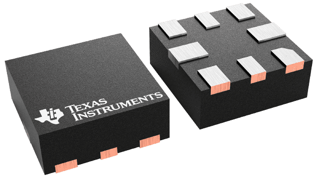
| Package / Case | 8-UFQFN |
| Package Length | 1.5 mm |
| Package Name | 8-UQFN |
| Package Width | 1.5 mm |
| Voltage - Supply (Maximum) | 3.6 V |
| Voltage - Supply (Minimum) | 0.8 V |
Pricing
Prices provided here are for design reference only. For realtime values and availability, please visit the distributors directly
Sign in to see pricing
Create a free account to access distributor pricing data.
CAD
3D models and CAD resources for this part
Documents
Technical documentation and resources