SN74AUP2G125 Series
2-ch, 0.8-V to 3.6-V low power buffers with 3-state outputs
Manufacturer: Texas Instruments
Catalog
2-ch, 0.8-V to 3.6-V low power buffers with 3-state outputs
Description
AI
The AUP family is TI’s premier solution to the industry’s low-power needs in battery-powered portable applications. This family ensures a very low static and dynamic power consumption across the entire VCCrange of 0.8 V to 3.6 V, resulting in an increased battery life. This product also maintains excellent signal integrity (see Figure 1 and Figure 2).
The SN74AUP2G125 is a dual bus buffer gate designed for 0.8-V to 3.6-V VCCoperation. This device features dual line drivers with 3-state outputs. Each output is disabled when the corresponding output-enable (OE) input is high. This device has the input-disable feature, which allows floating input signals.
To ensure the high-impedance state during power up or power down,OEshould be tied to VCCthrough a pullup resistor; the minimum value of the resistor is determined by the current-sinking capability of the driver.
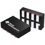
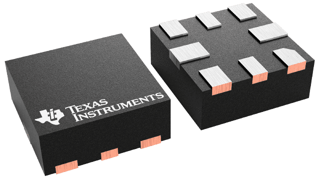
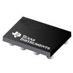
NanoStar™ package technology is a major breakthrough in IC packaging concepts, using the die as the package.
This device is fully specified for partial-power-down applications using Ioff. The Ioffcircuitry disables the outputs, preventing damaging current backflow through the device when it is powered down.
The AUP family is TI’s premier solution to the industry’s low-power needs in battery-powered portable applications. This family ensures a very low static and dynamic power consumption across the entire VCCrange of 0.8 V to 3.6 V, resulting in an increased battery life. This product also maintains excellent signal integrity (see Figure 1 and Figure 2).
The SN74AUP2G125 is a dual bus buffer gate designed for 0.8-V to 3.6-V VCCoperation. This device features dual line drivers with 3-state outputs. Each output is disabled when the corresponding output-enable (OE) input is high. This device has the input-disable feature, which allows floating input signals.
To ensure the high-impedance state during power up or power down,OEshould be tied to VCCthrough a pullup resistor; the minimum value of the resistor is determined by the current-sinking capability of the driver.
NanoStar™ package technology is a major breakthrough in IC packaging concepts, using the die as the package.
This device is fully specified for partial-power-down applications using Ioff. The Ioffcircuitry disables the outputs, preventing damaging current backflow through the device when it is powered down.