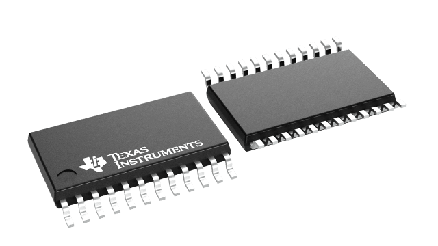
CDC2510CPWG4
UnknownIC PLL CLOCK DRIVER 24TSSOP
CDC2510CPWG4
UnknownIC PLL CLOCK DRIVER 24TSSOP
Description
General part information
CDC2510 Series
The CDC2510C is a high-performance, low-skew, low-jitter, phase-lock loop (PLL) clock driver. It uses a PLL to precisely align, in both frequency and phase, the feedback (FBOUT) output to the clock (CLK) input signal. It is specifically designed for use with synchronous DRAMs. The CDC2510C operates at VCC= 3.3 V . It also provides integrated series-damping resistors that make it ideal for driving point-to-point loads.
One bank of ten outputs provides ten low-skew, low-jitter copies of CLK. Output signal duty cycles are adjusted to 50 percent, independent of the duty cycle at CLK. All outputs can be enabled or disabled via a single output enable input. When the G input is high, the outputs switch in phase and frequency with CLK; when the G input is low, the outputs are disabled to the logic-low state.
Unlike many products containing PLLs, the CDC2510C does not require external RC networks. The loop filter for the PLL is included on-chip, minimizing component count, board space, and cost.
Technical Specifications
Parameters and characteristics for this part
| Specification | CDC2510CPWG4 |
|---|---|
| Differential Input | No |
| Differential Output | No |
| Divider | No |
| Frequency - Max | 125 MHz |
| Input | Clock |
| Input Ratio | 1 |
| Mounting Type | Surface Mount |
| Multiplier | No |
| Number of Circuits | 1 |
| Operating Temperature (Max) | 85 °C |
| Operating Temperature (Min) | 0 °C |
| Output | Clock |
| Output Ratio | 10 |
| Package Length | 0.173 in |
| Package Name | 24-TSSOP |
| Package Width | 4.4 mm |
| PLL | Yes with Bypass |
| Type | PLL Clock Driver |
| Voltage - Supply (Maximum) | 3.6 V |
| Voltage - Supply (Minimum) | 3 V |
Pricing
Prices provided here are for design reference only. For realtime values and availability, please visit the distributors directly
Sign in to see pricing
Create a free account to access distributor pricing data.
CAD
3D models and CAD resources for this part
Documents
Technical documentation and resources
No documents available