


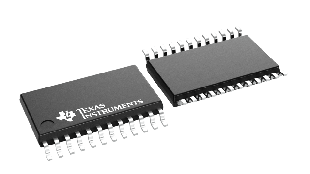
CDC2510 Series
3.3-V PLL clock driver with support for PC SDRAM registered DIMM design support document rev. 1.2
Manufacturer: Texas Instruments
Catalog
3.3-V PLL clock driver with support for PC SDRAM registered DIMM design support document rev. 1.2
Description
AI
The CDC2510C is a high-performance, low-skew, low-jitter, phase-lock loop (PLL) clock driver. It uses a PLL to precisely align, in both frequency and phase, the feedback (FBOUT) output to the clock (CLK) input signal. It is specifically designed for use with synchronous DRAMs. The CDC2510C operates at VCC= 3.3 V . It also provides integrated series-damping resistors that make it ideal for driving point-to-point loads.
One bank of ten outputs provides ten low-skew, low-jitter copies of CLK. Output signal duty cycles are adjusted to 50 percent, independent of the duty cycle at CLK. All outputs can be enabled or disabled via a single output enable input. When the G input is high, the outputs switch in phase and frequency with CLK; when the G input is low, the outputs are disabled to the logic-low state.
Unlike many products containing PLLs, the CDC2510C does not require external RC networks. The loop filter for the PLL is included on-chip, minimizing component count, board space, and cost.
Because it is based on PLL circuitry, the CDC2510C requires a stabilization time to achieve phase lock of the feedback signal to the reference signal. This stabilization time is required, following power up and application of a fixed-frequency, fixed-phase signal at CLK, and following any changes to the PLL reference or feedback signals. The PLL can be bypassed for test purposes by strapping AVCCto ground.
The CDC2510C is characterized for operation from 0°C to 85°C.
For application information refer to application reportsHigh Speed Distribution Design Techniques for CDC509/516/2509/2510/2516(literature number SLMA003) andUsing CDC2509A/2510A PLL with Spread Spectrum Clocking (SSC)(literature number SCAA039).
The CDC2510C is a high-performance, low-skew, low-jitter, phase-lock loop (PLL) clock driver. It uses a PLL to precisely align, in both frequency and phase, the feedback (FBOUT) output to the clock (CLK) input signal. It is specifically designed for use with synchronous DRAMs. The CDC2510C operates at VCC= 3.3 V . It also provides integrated series-damping resistors that make it ideal for driving point-to-point loads.
One bank of ten outputs provides ten low-skew, low-jitter copies of CLK. Output signal duty cycles are adjusted to 50 percent, independent of the duty cycle at CLK. All outputs can be enabled or disabled via a single output enable input. When the G input is high, the outputs switch in phase and frequency with CLK; when the G input is low, the outputs are disabled to the logic-low state.
Unlike many products containing PLLs, the CDC2510C does not require external RC networks. The loop filter for the PLL is included on-chip, minimizing component count, board space, and cost.
Because it is based on PLL circuitry, the CDC2510C requires a stabilization time to achieve phase lock of the feedback signal to the reference signal. This stabilization time is required, following power up and application of a fixed-frequency, fixed-phase signal at CLK, and following any changes to the PLL reference or feedback signals. The PLL can be bypassed for test purposes by strapping AVCCto ground.
The CDC2510C is characterized for operation from 0°C to 85°C.
For application information refer to application reportsHigh Speed Distribution Design Techniques for CDC509/516/2509/2510/2516(literature number SLMA003) andUsing CDC2509A/2510A PLL with Spread Spectrum Clocking (SSC)(literature number SCAA039).

