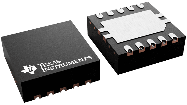
LM53601LQDSXRQ1
ActiveCONV DC-DC 3.55V TO 36V SYNCHRONOUS STEP DOWN SINGLE-OUT 5V 1A 10-PIN WSON EP T/R AUTOMOTIVE AEC-Q100
LM53601LQDSXRQ1
ActiveCONV DC-DC 3.55V TO 36V SYNCHRONOUS STEP DOWN SINGLE-OUT 5V 1A 10-PIN WSON EP T/R AUTOMOTIVE AEC-Q100
Description
General part information
LM53601-Q1 Series
The LM53600-Q1 and LM53601-Q1 synchronous buck regulator devices are optimized for automotive applications, providing an output voltage of 5 V, 3.3 V, or an adjustable output. Load current up to 650 mA is supported by the LM53600-Q1, while the LM53601-Q1 supports up to 1000 mA. Advanced high-speed circuitry allows the LM53600-Q1 and LM53601-Q1 devices to regulate from an input of 18 V to an output of 3.3 V at a fixed frequency of 2.1 MHz. Innovative architecture allows the device to regulate a 3.3-V output from an input voltage of only 3.8 V. The input voltage range up to 36 V, with transient tolerance of up to 42 V, eases input surge protection design. An open drain reset output, with filtering and delayed release, provides a true indication of system status. This feature negates the requirement for an additional supervisory component, saving cost and board space. Seamless transitions between PWM and PFM modes, along with a quiescent current of only 23 µA, ensures high efficiency and superior transient response at all loads. Few external components are needed allowing the generation of compact PCB layout. While the LM53600-Q1 and LM53601-Q1 devices are Q1 rated, electrical characteristics are ensured across a junction temperature range of –40°C up to 150°C.
The LM53600-Q1 and LM53601-Q1 synchronous buck regulator devices are optimized for automotive applications, providing an output voltage of 5 V, 3.3 V, or an adjustable output. Load current up to 650 mA is supported by the LM53600-Q1, while the LM53601-Q1 supports up to 1000 mA. Advanced high-speed circuitry allows the LM53600-Q1 and LM53601-Q1 devices to regulate from an input of 18 V to an output of 3.3 V at a fixed frequency of 2.1 MHz. Innovative architecture allows the device to regulate a 3.3-V output from an input voltage of only 3.8 V. The input voltage range up to 36 V, with transient tolerance of up to 42 V, eases input surge protection design. An open drain reset output, with filtering and delayed release, provides a true indication of system status. This feature negates the requirement for an additional supervisory component, saving cost and board space. Seamless transitions between PWM and PFM modes, along with a quiescent current of only 23 µA, ensures high efficiency and superior transient response at all loads. Few external components are needed allowing the generation of compact PCB layout. While the LM53600-Q1 and LM53601-Q1 devices are Q1 rated, electrical characteristics are ensured across a junction temperature range of –40°C up to 150°C.
Technical Specifications
Parameters and characteristics for this part
| Specification | LM53601LQDSXRQ1 |
|---|---|
| Current - Output | 1 A |
| Frequency - Switching | 2.1 MHz |
| Function | Step-Down |
| Grade | Automotive |
| Mounting Type | Surface Mount |
| Number of Outputs | 1 |
| Operating Temperature (Max) | 150 °C |
| Operating Temperature (Min) | -40 °C |
| Output Configuration | Positive |
| Output Type | Fixed |
| Package / Case | 10-WFDFN Exposed Pad |
| Package Length | 3 mm |
| Package Name | 10-WSON |
| Package Width | 3 mm |
| Qualification | AEC-Q100 |
| Synchronous Rectifier | Yes |
| Topology | Buck |
| Voltage - Input (Max) | 36 V |
| Voltage - Input (Min) | 3.8 V |
| Voltage - Output (Min/Fixed) | 5 V |
Pricing
Prices provided here are for design reference only. For realtime values and availability, please visit the distributors directly
Sign in to see pricing
Create a free account to access distributor pricing data.
CAD
3D models and CAD resources for this part
Documents
Technical documentation and resources