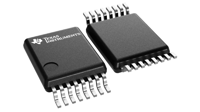
SN74LVC112ADGVR
ActiveTexas Instruments
DUAL NEGATIVE-EDGE-TRIGGERED J-K FLIP-FLOP WITH CLEAR AND PRESET
SN74LVC112ADGVR
ActiveTexas Instruments
DUAL NEGATIVE-EDGE-TRIGGERED J-K FLIP-FLOP WITH CLEAR AND PRESET
Description
General part information
74LVC112 Series
This dual negative-edge-triggered J-K flip-flop is designed for 1.65V to 3.6V VCC operation.
This dual negative-edge-triggered J-K flip-flop is designed for 1.65V to 3.6V VCC operation.
Technical Specifications
Parameters and characteristics for this part
| Specification | SN74LVC112ADGVR |
|---|---|
| Clock Frequency | 150 MHz |
| Current - Output High | 24 mA |
| Current - Output Low | 24 mA |
| Current - Quiescent (Iq) | 10 µA |
| Function | Set(Preset) and Reset |
| Input Capacitance | 4.5 pF |
| Max CL | 50 pF |
| Max Propagation Delay | 5.9 ns |
| Mounting Type | Surface Mount |
| Number of Bits per Element | 1 bits |
| Number of Elements | 2 |
| Operating Temperature (Max) | 85 °C |
| Operating Temperature (Min) | -40 °C |
| Output Type | Complementary |
| Package Length | 0.173 in |
| Package Name | 16-TFSOP, 16-TVSOP |
| Package Width | 4.4 mm |
| Trigger Type | Negative Edge |
| Type | JK Type |
| Voltage - Supply (Maximum) | 3.6 V |
| Voltage - Supply (Minimum) | 1.65 V |
Pricing
Prices provided here are for design reference only. For realtime values and availability, please visit the distributors directly
Sign in to see pricing
Create a free account to access distributor pricing data.
CAD
3D models and CAD resources for this part
Documents
Technical documentation and resources
Migration From 3.3-V To 2.5-V Power Supplies For Logic Devices
Input and Output Characteristics of Digital Integrated Circuits
Selecting the Right Level Translation Solution (Rev. A)
Bus-Interface Devices With Output-Damping Resistors Or Reduced-Drive Outputs (Rev. A)
Standard Linear & Logic for PCs, Servers & Motherboards
Implications of Slow or Floating CMOS Inputs (Rev. E)
How to Select Little Logic (Rev. A)
Signal Switch Data Book (Rev. A)
Little Logic Guide 2018 (Rev. G)
Low-Voltage Logic (LVC) Designer's Guide
STANDARD LINEAR AND LOGIC FOR DVD/VCD PLAYERS
Texas Instruments Little Logic Application Report
Live Insertion
LVC Characterization Information
Power-Up Behavior of Clocked Devices (Rev. B)
SN74LVC112A Dual Negative-Edge-Triggered J-K Flip-Flop With Clear and Preset datasheet (Rev. N)
Logic Guide (Rev. AB)
Understanding Advanced Bus-Interface Products Design Guide
Understanding and Interpreting Standard-Logic Data Sheets (Rev. C)
LVC and LV Low-Voltage CMOS Logic Data Book (Rev. B)
CMOS Power Consumption and CPD Calculation (Rev. B)
16-Bit Widebus Logic Families in 56-Ball, 0.65-mm Pitch Very Thin Fine-Pitch BGA (Rev. B)
TI IBIS File Creation, Validation, and Distribution Processes
LOGIC Pocket Data Book (Rev. B)
Design Summary for WCSP Little Logic (Rev. B)
Power-Up 3-State (PU3S) Circuits in TI Standard Logic Devices
Semiconductor Packing Material Electrostatic Discharge (ESD) Protection
Use of the CMOS Unbuffered Inverter in Oscillator Circuits
SN74LVC112ADGVR | Datasheet