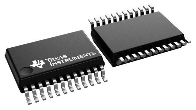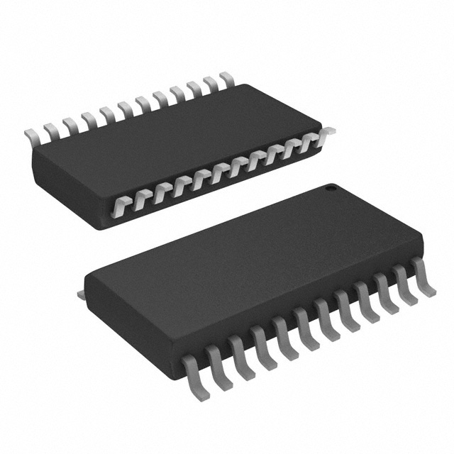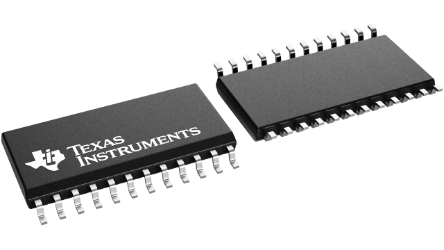
CDC351IDWG4
UnknownIC CLK BUFFER 1:10 100MHZ 24SOIC
CDC351IDWG4
UnknownIC CLK BUFFER 1:10 100MHZ 24SOIC
Description
General part information
CDC351 Series
The CDC351 is a high-performance clock-driver circuit that distributes one input (A) to ten outputs (Y) with minimum skew for clock distribution. The output-enable (OE)\ input disables the outputs to a high-impedance state. The CDC351 operates at nominal 3.3-V VCC.
The propagation delays are adjusted at the factory using the P0 and P1 pins. The factory adjustments ensure that the part-to-part skew is minimized and is kept within a specified window. Pins P0 and P1 are not intended for customer use and should be connected to GND.
The CDC351 is a high-performance clock-driver circuit that distributes one input (A) to ten outputs (Y) with minimum skew for clock distribution. The output-enable (OE)\ input disables the outputs to a high-impedance state. The CDC351 operates at nominal 3.3-V VCC.
Technical Specifications
Parameters and characteristics for this part
| Specification | CDC351IDWG4 |
|---|---|
| Differential Input | No |
| Differential Output | No |
| Frequency - Max | 100 MHz |
| Input | LVTTL |
| Input Ratio | 1 |
| Mounting Type | Surface Mount |
| Number of Circuits | 1 |
| Operating Temperature (Max) | 85 °C |
| Operating Temperature (Min) | -40 °C |
| Output | TRI-State, LVTTL |
| Output Ratio | 10 |
| Package Length | 0.295 in |
| Package Name | 24-SOIC |
| Package Width | 7.5 mm |
| Type | Fanout Buffer (Distribution) |
| Voltage - Supply (Maximum) | 3.6 V |
| Voltage - Supply (Minimum) | 3 V |
Pricing
Prices provided here are for design reference only. For realtime values and availability, please visit the distributors directly
Sign in to see pricing
Create a free account to access distributor pricing data.
CAD
3D models and CAD resources for this part
Documents
Technical documentation and resources
No documents available