ADC12C105CISQE/NOPB
Active12-BIT, 105-MSPS, 1.0-GHZ INPUT BANDWIDTH ANALOG-TO-DIGITAL CONVERTER (ADC)
Deep-Dive with AI
Search across all available documentation for this part.
ADC12C105CISQE/NOPB
Active12-BIT, 105-MSPS, 1.0-GHZ INPUT BANDWIDTH ANALOG-TO-DIGITAL CONVERTER (ADC)
Technical Specifications
Parameters and characteristics commom to parts in this series
| Specification | ADC12C105CISQE/NOPB | ADC12C105 Series |
|---|---|---|
| Architecture | Pipelined | Pipelined |
| Configuration | S/H-ADC | S/H-ADC |
| Data Interface | Parallel | Parallel |
| Input Type | Differential | Differential |
| Mounting Type | Surface Mount | Surface Mount |
| Number of A/D Converters | 1 | 1 |
| Number of Bits | 12 | 12 |
| Number of Inputs | 1 | 1 |
| Operating Temperature [Max] | 85 °C | 85 °C |
| Operating Temperature [Min] | -40 °C | -40 °C |
| Ratio - S/H:ADC | 1:1 | 1:1 |
| Reference Type | Internal, External | Internal, External |
| Sampling Rate (Per Second) | 105 M | 105 M |
| Supplier Device Package | 32-WQFN (5x5) | 32-WQFN (5x5) |
| Voltage - Supply, Analog [Max] | 3.6 V | 3.6 V |
| Voltage - Supply, Analog [Min] | 2.7 V | 2.7 V |
| Voltage - Supply, Digital [Max] | 3.6 V | 3.6 V |
| Voltage - Supply, Digital [Min] | 2.4 V | 2.4 V |
Pricing
Prices provided here are for design reference only. For realtime values and availability, please visit the distributors directly
ADC12C105 Series
12-Bit, 105-MSPS, 1.0-GHz Input Bandwidth Analog-to-Digital Converter (ADC)
| Part | Mounting Type | Number of Inputs | Data Interface | Voltage - Supply, Analog [Min] | Voltage - Supply, Analog [Max] | Operating Temperature [Min] | Operating Temperature [Max] | Number of Bits | Architecture | Voltage - Supply, Digital [Max] | Voltage - Supply, Digital [Min] | Ratio - S/H:ADC | Supplier Device Package | Reference Type | Sampling Rate (Per Second) | Configuration | Input Type | Number of A/D Converters |
|---|---|---|---|---|---|---|---|---|---|---|---|---|---|---|---|---|---|---|
Texas Instruments ADC12C105CISQE/NOPBThe ADC12C105 is a high-performance CMOS analog-to-digital converter capable of converting analog input signals into 12-bit digital words at rates up to 105 Mega Samples Per Second (MSPS). This converter uses a differential, pipelined architecture with digital error correction and an on-chip sample-and-hold circuit to minimize power consumption and the external component count, while providing excellent dynamic performance. A unique sample-and-hold stage yields a full-power bandwidth of 1 GHz. The ADC12C105 may be operated from a single +3.0V or +3.3V power supply and consumes low power.
A separate +2.5V supply may be used for the digital output interface which allows lower power operation with reduced noise. A power-down feature reduces the power consumption to very low levels while still allowing fast wake-up time to full operation. The differential inputs accept a 2V full scale differential input swing. A stable 1.2V internal voltage reference is provided, or the ADC12C105 can be operated with an external 1.2V reference. Output data format (offset binary versus 2's complement) and duty cycle stabilizer are pin-selectable. The duty cycle stabilizer maintains performance over a wide range of clock duty cycles.
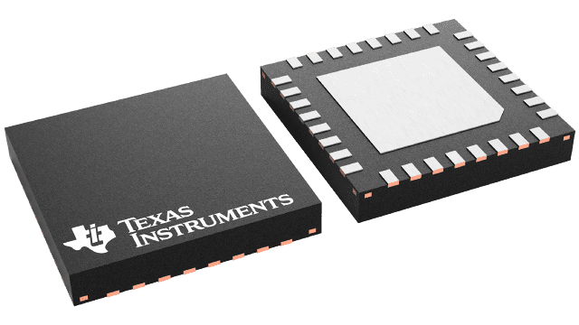
The ADC12C105 is available in a 32-lead WQFN package and operates over the industrial temperature range of −40°C to +85°C.
The ADC12C105 is a high-performance CMOS analog-to-digital converter capable of converting analog input signals into 12-bit digital words at rates up to 105 Mega Samples Per Second (MSPS). This converter uses a differential, pipelined architecture with digital error correction and an on-chip sample-and-hold circuit to minimize power consumption and the external component count, while providing excellent dynamic performance. A unique sample-and-hold stage yields a full-power bandwidth of 1 GHz. The ADC12C105 may be operated from a single +3.0V or +3.3V power supply and consumes low power.
A separate +2.5V supply may be used for the digital output interface which allows lower power operation with reduced noise. A power-down feature reduces the power consumption to very low levels while still allowing fast wake-up time to full operation. The differential inputs accept a 2V full scale differential input swing. A stable 1.2V internal voltage reference is provided, or the ADC12C105 can be operated with an external 1.2V reference. Output data format (offset binary versus 2's complement) and duty cycle stabilizer are pin-selectable. The duty cycle stabilizer maintains performance over a wide range of clock duty cycles.
The ADC12C105 is available in a 32-lead WQFN package and operates over the industrial temperature range of −40°C to +85°C. | Surface Mount | 1 | Parallel | 2.7 V | 3.6 V | -40 °C | 85 °C | 12 | Pipelined | 3.6 V | 2.4 V | 1:1 | 32-WQFN (5x5) | External, Internal | 105 M | S/H-ADC | Differential | 1 |
Texas Instruments ADC12C105CISQ/NOPBThe ADC12C105 is a high-performance CMOS analog-to-digital converter capable of converting analog input signals into 12-bit digital words at rates up to 105 Mega Samples Per Second (MSPS). This converter uses a differential, pipelined architecture with digital error correction and an on-chip sample-and-hold circuit to minimize power consumption and the external component count, while providing excellent dynamic performance. A unique sample-and-hold stage yields a full-power bandwidth of 1 GHz. The ADC12C105 may be operated from a single +3.0V or +3.3V power supply and consumes low power.
A separate +2.5V supply may be used for the digital output interface which allows lower power operation with reduced noise. A power-down feature reduces the power consumption to very low levels while still allowing fast wake-up time to full operation. The differential inputs accept a 2V full scale differential input swing. A stable 1.2V internal voltage reference is provided, or the ADC12C105 can be operated with an external 1.2V reference. Output data format (offset binary versus 2's complement) and duty cycle stabilizer are pin-selectable. The duty cycle stabilizer maintains performance over a wide range of clock duty cycles.
The ADC12C105 is available in a 32-lead WQFN package and operates over the industrial temperature range of −40°C to +85°C.
The ADC12C105 is a high-performance CMOS analog-to-digital converter capable of converting analog input signals into 12-bit digital words at rates up to 105 Mega Samples Per Second (MSPS). This converter uses a differential, pipelined architecture with digital error correction and an on-chip sample-and-hold circuit to minimize power consumption and the external component count, while providing excellent dynamic performance. A unique sample-and-hold stage yields a full-power bandwidth of 1 GHz. The ADC12C105 may be operated from a single +3.0V or +3.3V power supply and consumes low power.
A separate +2.5V supply may be used for the digital output interface which allows lower power operation with reduced noise. A power-down feature reduces the power consumption to very low levels while still allowing fast wake-up time to full operation. The differential inputs accept a 2V full scale differential input swing. A stable 1.2V internal voltage reference is provided, or the ADC12C105 can be operated with an external 1.2V reference. Output data format (offset binary versus 2's complement) and duty cycle stabilizer are pin-selectable. The duty cycle stabilizer maintains performance over a wide range of clock duty cycles.
The ADC12C105 is available in a 32-lead WQFN package and operates over the industrial temperature range of −40°C to +85°C. | Surface Mount | 1 | Parallel | 2.7 V | 3.6 V | -40 °C | 85 °C | 12 | Pipelined | 3.6 V | 2.4 V | 1:1 | 32-WQFN (5x5) | External, Internal | 105 M | S/H-ADC | Differential | 1 |
Description
General part information
ADC12C105 Series
The ADC12C105 is a high-performance CMOS analog-to-digital converter capable of converting analog input signals into 12-bit digital words at rates up to 105 Mega Samples Per Second (MSPS). This converter uses a differential, pipelined architecture with digital error correction and an on-chip sample-and-hold circuit to minimize power consumption and the external component count, while providing excellent dynamic performance. A unique sample-and-hold stage yields a full-power bandwidth of 1 GHz. The ADC12C105 may be operated from a single +3.0V or +3.3V power supply and consumes low power.
A separate +2.5V supply may be used for the digital output interface which allows lower power operation with reduced noise. A power-down feature reduces the power consumption to very low levels while still allowing fast wake-up time to full operation. The differential inputs accept a 2V full scale differential input swing. A stable 1.2V internal voltage reference is provided, or the ADC12C105 can be operated with an external 1.2V reference. Output data format (offset binary versus 2's complement) and duty cycle stabilizer are pin-selectable. The duty cycle stabilizer maintains performance over a wide range of clock duty cycles.
The ADC12C105 is available in a 32-lead WQFN package and operates over the industrial temperature range of −40°C to +85°C.