CDC2351DB
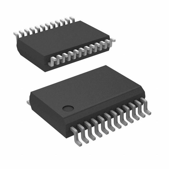
Active1-LINE TO 10-LINE CLOCK DRIVER WITH 3-STATE OUTPUTS 24-SSOP 0 TO 70
Deep-Dive with AI
Search across all available documentation for this part.
CDC2351DB
Active1-LINE TO 10-LINE CLOCK DRIVER WITH 3-STATE OUTPUTS 24-SSOP 0 TO 70
Deep-Dive with AI
Technical Specifications
Parameters and characteristics commom to parts in this series
| Specification | CDC2351DB | CDC2351 Series |
|---|---|---|
| Differential - Input:Output [custom] | False | False |
| Differential - Input:Output [custom] | False | False |
| Frequency - Max [Max] | 100 MHz | 100 MHz |
| Grade | - | Automotive |
| Mounting Type | Surface Mount | Surface Mount |
| Number of Circuits | 1 | 1 |
| Operating Temperature [Max] | 70 ░C | 70 - 125 ░C |
| Operating Temperature [Min] | 0 °C | -55 - 0 °C |
| Output | LVTTL | LVTTL |
| Package / Case | 0.209 in | 0.209 in |
| Package / Case | 5.3 mm | 5.3 mm |
| Package / Case | 24-SSOP | 24-SOIC, 24-SSOP |
| Package / Case | - | 7.5 mm |
| Package / Case | - | 0.295 in |
| Qualification | - | AEC-Q100 |
| Ratio - Input:Output [custom] | 1 | 1 |
| Ratio - Input:Output [custom] | 10 | 10 |
| Supplier Device Package | 24-SSOP | 24-SOIC, 24-SSOP |
| Type | Fanout Buffer (Distribution) | Fanout Buffer (Distribution) |
| Voltage - Supply [Max] | 3.6 V | 3.6 V |
| Voltage - Supply [Min] | 3 V | 3 V |
Pricing
Prices provided here are for design reference only. For realtime values and availability, please visit the distributors directly
CDC2351 Series
Automotive 1-line to 10-line clock driver with 3-state outputs
| Part | Supplier Device Package | Package / Case [y] | Package / Case [x] | Package / Case | Operating Temperature [Max] | Operating Temperature [Min] | Number of Circuits | Voltage - Supply [Max] | Voltage - Supply [Min] | Differential - Input:Output [custom] | Differential - Input:Output [custom] | Mounting Type | Ratio - Input:Output [custom] | Ratio - Input:Output [custom] | Frequency - Max [Max] | Type | Output | Package / Case | Package / Case | Grade | Qualification |
|---|---|---|---|---|---|---|---|---|---|---|---|---|---|---|---|---|---|---|---|---|---|
Texas Instruments CDC2351DWRThe CDC2351 is a high-performance clock-driver circuit that distributes one input (A) to ten outputs (Y) with minimum skew for clock distribution. The output-enable (OE\) input disables the outputs to a high-impedance state. Each output has an internal series damping resistor to improve signal integrity at the load. The CDC2351 operates at nominal 3.3-V VCC.
The propagation delays are adjusted at the factory using the P0 and P1 pins. The factory adjustments ensure that the part-to-part skew is minimized and is kept within a specified window. Pins P0 and P1 are not intended for customer use and should be connected to GND.
The CDC2351 is characterized for operation from 0°C to 70°C. The CDC2351Q is characterized for operation over the full automotive temperature range of -40°C to 125°C.
The CDC2351 is a high-performance clock-driver circuit that distributes one input (A) to ten outputs (Y) with minimum skew for clock distribution. The output-enable (OE\) input disables the outputs to a high-impedance state. Each output has an internal series damping resistor to improve signal integrity at the load. The CDC2351 operates at nominal 3.3-V VCC.
The propagation delays are adjusted at the factory using the P0 and P1 pins. The factory adjustments ensure that the part-to-part skew is minimized and is kept within a specified window. Pins P0 and P1 are not intended for customer use and should be connected to GND.
The CDC2351 is characterized for operation from 0°C to 70°C. The CDC2351Q is characterized for operation over the full automotive temperature range of -40°C to 125°C. | 24-SOIC | 7.5 mm | 0.295 in | 24-SOIC | 70 ░C | 0 °C | 1 | 3.6 V | 3 V | Surface Mount | 1 | 10 | 100 MHz | Fanout Buffer (Distribution) | LVTTL | ||||||
Texas Instruments CDC2351MDBREPThe CDC2351 is a high-performance clock-driver circuit that distributes one input (A) to 10 outputs (Y) with minimum skew for clock distribution. The output-enable (OE)\ input disables the outputs to a high-impedance state. Each output has an internal series damping resistor to improve signal integrity at the load. The CDC2351 operates at nominal 3.3-V VCC.
The propagation delays are adjusted at the factory using the P0 and P1 pins. The factory adjustments ensure that the part-to-part skew is minimized and is kept within a specified window. Pins P0 and P1 are not intended for customer use and should be connected to GND.
The CDC2351M is characterized for operation over the full military temperature range of –55°C to 125°C.
The CDC2351 is a high-performance clock-driver circuit that distributes one input (A) to 10 outputs (Y) with minimum skew for clock distribution. The output-enable (OE)\ input disables the outputs to a high-impedance state. Each output has an internal series damping resistor to improve signal integrity at the load. The CDC2351 operates at nominal 3.3-V VCC.
The propagation delays are adjusted at the factory using the P0 and P1 pins. The factory adjustments ensure that the part-to-part skew is minimized and is kept within a specified window. Pins P0 and P1 are not intended for customer use and should be connected to GND.
The CDC2351M is characterized for operation over the full military temperature range of –55°C to 125°C. | 24-SSOP | 24-SSOP | 125 °C | -55 °C | 1 | 3.6 V | 3 V | Surface Mount | 1 | 10 | 100 MHz | Fanout Buffer (Distribution) | LVTTL | 0.209 in | 5.3 mm | ||||||
Texas Instruments CDC2351DBRG4Clock Fanout Buffer (Distribution) IC 1:10 100 MHz 24-SSOP (0.209", 5.30mm Width) | 24-SSOP | 24-SSOP | 70 ░C | 0 °C | 1 | 3.6 V | 3 V | Surface Mount | 1 | 10 | 100 MHz | Fanout Buffer (Distribution) | LVTTL | 0.209 in | 5.3 mm | ||||||
Texas Instruments CDC2351DBThe CDC2351 is a high-performance clock-driver circuit that distributes one input (A) to ten outputs (Y) with minimum skew for clock distribution. The output-enable (OE\) input disables the outputs to a high-impedance state. Each output has an internal series damping resistor to improve signal integrity at the load. The CDC2351 operates at nominal 3.3-V VCC.
The propagation delays are adjusted at the factory using the P0 and P1 pins. The factory adjustments ensure that the part-to-part skew is minimized and is kept within a specified window. Pins P0 and P1 are not intended for customer use and should be connected to GND.
The CDC2351 is characterized for operation from 0°C to 70°C. The CDC2351Q is characterized for operation over the full automotive temperature range of -40°C to 125°C.
The CDC2351 is a high-performance clock-driver circuit that distributes one input (A) to ten outputs (Y) with minimum skew for clock distribution. The output-enable (OE\) input disables the outputs to a high-impedance state. Each output has an internal series damping resistor to improve signal integrity at the load. The CDC2351 operates at nominal 3.3-V VCC.
The propagation delays are adjusted at the factory using the P0 and P1 pins. The factory adjustments ensure that the part-to-part skew is minimized and is kept within a specified window. Pins P0 and P1 are not intended for customer use and should be connected to GND.
The CDC2351 is characterized for operation from 0°C to 70°C. The CDC2351Q is characterized for operation over the full automotive temperature range of -40°C to 125°C. | 24-SSOP | 24-SSOP | 70 ░C | 0 °C | 1 | 3.6 V | 3 V | Surface Mount | 1 | 10 | 100 MHz | Fanout Buffer (Distribution) | LVTTL | 0.209 in | 5.3 mm | ||||||
Texas Instruments CDC2351QDBRG4The CDC2351 is a high-performance clock-driver circuit that distributes one input (A) to ten outputs (Y) with minimum skew for clock distribution. The output-enable (OE\) input disables the outputs to a high-impedance state. Each output has an internal series damping resistor to improve signal integrity at the load. The CDC2351 operates at nominal 3.3-V VCC.
The propagation delays are adjusted at the factory using the P0 and P1 pins. The factory adjustments ensure that the part-to-part skew is minimized and is kept within a specified window. Pins P0 and P1 are not intended for customer use and should be connected to GND.
The CDC2351 is characterized for operation from 0°C to 70°C. The CDC2351Q is characterized for operation over the full automotive temperature range of -40°C to 125°C.
The CDC2351 is a high-performance clock-driver circuit that distributes one input (A) to ten outputs (Y) with minimum skew for clock distribution. The output-enable (OE\) input disables the outputs to a high-impedance state. Each output has an internal series damping resistor to improve signal integrity at the load. The CDC2351 operates at nominal 3.3-V VCC.
The propagation delays are adjusted at the factory using the P0 and P1 pins. The factory adjustments ensure that the part-to-part skew is minimized and is kept within a specified window. Pins P0 and P1 are not intended for customer use and should be connected to GND.
The CDC2351 is characterized for operation from 0°C to 70°C. The CDC2351Q is characterized for operation over the full automotive temperature range of -40°C to 125°C. | 24-SSOP | 24-SSOP | 125 °C | -40 °C | 1 | 3.6 V | 3 V | Surface Mount | 1 | 10 | 100 MHz | Fanout Buffer (Distribution) | LVTTL | 0.209 in | 5.3 mm | Automotive | AEC-Q100 | ||||
Texas Instruments CDC2351DBRThe CDC2351 is a high-performance clock-driver circuit that distributes one input (A) to ten outputs (Y) with minimum skew for clock distribution. The output-enable (OE\) input disables the outputs to a high-impedance state. Each output has an internal series damping resistor to improve signal integrity at the load. The CDC2351 operates at nominal 3.3-V VCC.
The propagation delays are adjusted at the factory using the P0 and P1 pins. The factory adjustments ensure that the part-to-part skew is minimized and is kept within a specified window. Pins P0 and P1 are not intended for customer use and should be connected to GND.
The CDC2351 is characterized for operation from 0°C to 70°C. The CDC2351Q is characterized for operation over the full automotive temperature range of -40°C to 125°C.
The CDC2351 is a high-performance clock-driver circuit that distributes one input (A) to ten outputs (Y) with minimum skew for clock distribution. The output-enable (OE\) input disables the outputs to a high-impedance state. Each output has an internal series damping resistor to improve signal integrity at the load. The CDC2351 operates at nominal 3.3-V VCC.
The propagation delays are adjusted at the factory using the P0 and P1 pins. The factory adjustments ensure that the part-to-part skew is minimized and is kept within a specified window. Pins P0 and P1 are not intended for customer use and should be connected to GND.
The CDC2351 is characterized for operation from 0°C to 70°C. The CDC2351Q is characterized for operation over the full automotive temperature range of -40°C to 125°C. | 24-SSOP | 24-SSOP | 70 ░C | 0 °C | 1 | 3.6 V | 3 V | Surface Mount | 1 | 10 | 100 MHz | Fanout Buffer (Distribution) | LVTTL | 0.209 in | 5.3 mm | ||||||
Texas Instruments CDC2351QDBG4The CDC2351 is a high-performance clock-driver circuit that distributes one input (A) to ten outputs (Y) with minimum skew for clock distribution. The output-enable (OE\) input disables the outputs to a high-impedance state. Each output has an internal series damping resistor to improve signal integrity at the load. The CDC2351 operates at nominal 3.3-V VCC.
The propagation delays are adjusted at the factory using the P0 and P1 pins. The factory adjustments ensure that the part-to-part skew is minimized and is kept within a specified window. Pins P0 and P1 are not intended for customer use and should be connected to GND.
The CDC2351 is characterized for operation from 0°C to 70°C. The CDC2351Q is characterized for operation over the full automotive temperature range of -40°C to 125°C.
The CDC2351 is a high-performance clock-driver circuit that distributes one input (A) to ten outputs (Y) with minimum skew for clock distribution. The output-enable (OE\) input disables the outputs to a high-impedance state. Each output has an internal series damping resistor to improve signal integrity at the load. The CDC2351 operates at nominal 3.3-V VCC.
The propagation delays are adjusted at the factory using the P0 and P1 pins. The factory adjustments ensure that the part-to-part skew is minimized and is kept within a specified window. Pins P0 and P1 are not intended for customer use and should be connected to GND.
The CDC2351 is characterized for operation from 0°C to 70°C. The CDC2351Q is characterized for operation over the full automotive temperature range of -40°C to 125°C. | 24-SSOP | 24-SSOP | 125 °C | -40 °C | 1 | 3.6 V | 3 V | Surface Mount | 1 | 10 | 100 MHz | Fanout Buffer (Distribution) | LVTTL | 0.209 in | 5.3 mm | Automotive | AEC-Q100 | ||||
Texas Instruments CDC2351QDBRThe CDC2351 is a high-performance clock-driver circuit that distributes one input (A) to ten outputs (Y) with minimum skew for clock distribution. The output-enable (OE\) input disables the outputs to a high-impedance state. Each output has an internal series damping resistor to improve signal integrity at the load. The CDC2351 operates at nominal 3.3-V VCC.
The propagation delays are adjusted at the factory using the P0 and P1 pins. The factory adjustments ensure that the part-to-part skew is minimized and is kept within a specified window. Pins P0 and P1 are not intended for customer use and should be connected to GND.
The CDC2351 is characterized for operation from 0°C to 70°C. The CDC2351Q is characterized for operation over the full automotive temperature range of -40°C to 125°C.
The CDC2351 is a high-performance clock-driver circuit that distributes one input (A) to ten outputs (Y) with minimum skew for clock distribution. The output-enable (OE\) input disables the outputs to a high-impedance state. Each output has an internal series damping resistor to improve signal integrity at the load. The CDC2351 operates at nominal 3.3-V VCC.
The propagation delays are adjusted at the factory using the P0 and P1 pins. The factory adjustments ensure that the part-to-part skew is minimized and is kept within a specified window. Pins P0 and P1 are not intended for customer use and should be connected to GND.
The CDC2351 is characterized for operation from 0°C to 70°C. The CDC2351Q is characterized for operation over the full automotive temperature range of -40°C to 125°C. | 24-SSOP | 24-SSOP | 125 °C | -40 °C | 1 | 3.6 V | 3 V | Surface Mount | 1 | 10 | 100 MHz | Fanout Buffer (Distribution) | LVTTL | 0.209 in | 5.3 mm | Automotive | AEC-Q100 | ||||
Texas Instruments CDC2351QDBThe CDC2351 is a high-performance clock-driver circuit that distributes one input (A) to ten outputs (Y) with minimum skew for clock distribution. The output-enable (OE\) input disables the outputs to a high-impedance state. Each output has an internal series damping resistor to improve signal integrity at the load. The CDC2351 operates at nominal 3.3-V VCC.
The propagation delays are adjusted at the factory using the P0 and P1 pins. The factory adjustments ensure that the part-to-part skew is minimized and is kept within a specified window. Pins P0 and P1 are not intended for customer use and should be connected to GND.
The CDC2351 is characterized for operation from 0°C to 70°C. The CDC2351Q is characterized for operation over the full automotive temperature range of -40°C to 125°C.
The CDC2351 is a high-performance clock-driver circuit that distributes one input (A) to ten outputs (Y) with minimum skew for clock distribution. The output-enable (OE\) input disables the outputs to a high-impedance state. Each output has an internal series damping resistor to improve signal integrity at the load. The CDC2351 operates at nominal 3.3-V VCC.
The propagation delays are adjusted at the factory using the P0 and P1 pins. The factory adjustments ensure that the part-to-part skew is minimized and is kept within a specified window. Pins P0 and P1 are not intended for customer use and should be connected to GND.
The CDC2351 is characterized for operation from 0°C to 70°C. The CDC2351Q is characterized for operation over the full automotive temperature range of -40°C to 125°C. | 24-SSOP | 24-SSOP | 125 °C | -40 °C | 1 | 3.6 V | 3 V | Surface Mount | 1 | 10 | 100 MHz | Fanout Buffer (Distribution) | LVTTL | 0.209 in | 5.3 mm | Automotive | AEC-Q100 | ||||
Texas Instruments CDC2351DWRG4Clock Fanout Buffer (Distribution) IC 1:10 100 MHz 24-SOIC (0.295", 7.50mm Width) | 24-SOIC | 7.5 mm | 0.295 in | 24-SOIC | 70 ░C | 0 °C | 1 | 3.6 V | 3 V | Surface Mount | 1 | 10 | 100 MHz | Fanout Buffer (Distribution) | LVTTL | ||||||
Texas Instruments CDC2351DWThe CDC2351 is a high-performance clock-driver circuit that distributes one input (A) to ten outputs (Y) with minimum skew for clock distribution. The output-enable (OE\) input disables the outputs to a high-impedance state. Each output has an internal series damping resistor to improve signal integrity at the load. The CDC2351 operates at nominal 3.3-V VCC.
The propagation delays are adjusted at the factory using the P0 and P1 pins. The factory adjustments ensure that the part-to-part skew is minimized and is kept within a specified window. Pins P0 and P1 are not intended for customer use and should be connected to GND.
The CDC2351 is characterized for operation from 0°C to 70°C. The CDC2351Q is characterized for operation over the full automotive temperature range of -40°C to 125°C.
The CDC2351 is a high-performance clock-driver circuit that distributes one input (A) to ten outputs (Y) with minimum skew for clock distribution. The output-enable (OE\) input disables the outputs to a high-impedance state. Each output has an internal series damping resistor to improve signal integrity at the load. The CDC2351 operates at nominal 3.3-V VCC.
The propagation delays are adjusted at the factory using the P0 and P1 pins. The factory adjustments ensure that the part-to-part skew is minimized and is kept within a specified window. Pins P0 and P1 are not intended for customer use and should be connected to GND.
The CDC2351 is characterized for operation from 0°C to 70°C. The CDC2351Q is characterized for operation over the full automotive temperature range of -40°C to 125°C. | 24-SOIC | 7.5 mm | 0.295 in | 24-SOIC | 70 ░C | 0 °C | 1 | 3.6 V | 3 V | Surface Mount | 1 | 10 | 100 MHz | Fanout Buffer (Distribution) | LVTTL |
Description
General part information
CDC2351 Series
The CDC2351 is a high-performance clock-driver circuit that distributes one input (A) to ten outputs (Y) with minimum skew for clock distribution. The output-enable (OE\) input disables the outputs to a high-impedance state. Each output has an internal series damping resistor to improve signal integrity at the load. The CDC2351 operates at nominal 3.3-V VCC.
The propagation delays are adjusted at the factory using the P0 and P1 pins. The factory adjustments ensure that the part-to-part skew is minimized and is kept within a specified window. Pins P0 and P1 are not intended for customer use and should be connected to GND.
The CDC2351 is characterized for operation from 0°C to 70°C. The CDC2351Q is characterized for operation over the full automotive temperature range of -40°C to 125°C.
Documents
Technical documentation and resources