CDCEL913PW
ActiveCLOCK SYNTHESIZER / JITTER CLEANER PROGRAMMABLE 1-PLL V CXO CLOCK SYNTH A 595-CDCEL913PWR
CDCEL913PW
ActiveCLOCK SYNTHESIZER / JITTER CLEANER PROGRAMMABLE 1-PLL V CXO CLOCK SYNTH A 595-CDCEL913PWR
Description
General part information
CDCEL913 Series
The CDCE913 and CDCEL913 devices are modular PLL-based, low-cost, high-performance, programmable clock synthesizers. The devices generate up to three output clocks from a single input frequency. Each output can be programmed in-system for any clock frequency up to 230MHz, using the integrated configurable PLL.
The CDCx913 has separate output supply pins, VDDOUT, which is 1.8V for CDCEL913 and 2.5V to 3.3V for CDCE913.
The input accepts an external crystal or LVCMOS clock signal. A selectable on-chip VCXO allows synchronization of the output frequency to an external control signal.
Technical Specifications
Parameters and characteristics for this part
| Specification | CDCEL913PW |
|---|---|
| Differential Input | No |
| Differential Output | No |
| Divider | Yes |
| Frequency - Max | 230 MHz |
| Input | LVCMOS, Crystal |
| Input Ratio | 1 |
| Mounting Type | Surface Mount |
| Multiplier | Yes |
| Number of Circuits | 1 |
| Operating Temperature (Max) | 85 °C |
| Operating Temperature (Min) | -40 °C |
| Output | LVCMOS |
| Output Ratio | 3 |
| Package Length | 0.173 in |
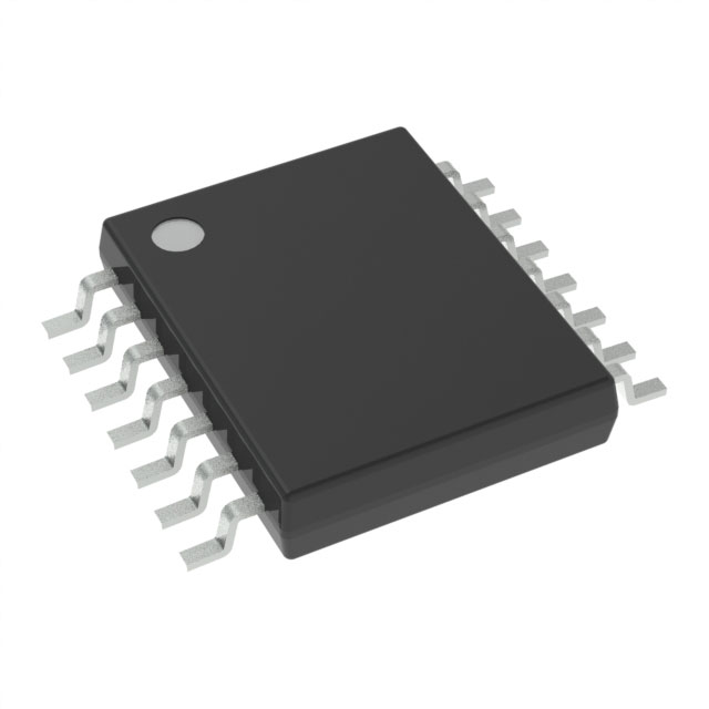
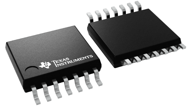
| Package Name | 14-TSSOP |
| Package Width | 4.4 mm |
| PLL | Yes with Bypass |
| Type | PLL Clock Synthesizer |
| Voltage - Supply (Maximum) | 1.9 V |
| Voltage - Supply (Minimum) | 1.7 V |
Pricing
Prices provided here are for design reference only. For realtime values and availability, please visit the distributors directly
Sign in to see pricing
Create a free account to access distributor pricing data.
CAD
3D models and CAD resources for this part
Documents
Technical documentation and resources