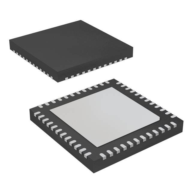
CDCE62005RGZT
Active5/10 OUTPUTS CLOCK GENERATOR/JITTER CLEANER WITH INTEGRATED DUAL VCO 48-VQFN -40 TO 85
Deep-Dive with AI
Search across all available documentation for this part.

CDCE62005RGZT
Active5/10 OUTPUTS CLOCK GENERATOR/JITTER CLEANER WITH INTEGRATED DUAL VCO 48-VQFN -40 TO 85
Technical Specifications
Parameters and characteristics commom to parts in this series
| Specification | CDCE62005RGZT | CDCE62005 Series |
|---|---|---|
| Differential - Input:Output [custom] | True | True |
| Differential - Input:Output [custom] | True | True |
| Divider/Multiplier | Yes/No | Yes/No |
| Frequency - Max [Max] | 1.5 GHz | 1.5 GHz |
| Input | LVDS, LVPECL, LVCMOS, Crystal | LVDS, LVPECL, LVCMOS, Crystal |
| Mounting Type | Surface Mount | Surface Mount |
| Number of Circuits | 1 | 1 |
| Operating Temperature [Max] | 85 °C | 85 °C |
| Operating Temperature [Min] | -40 °C | -40 °C |
| Output | LVPECL, LVCMOS, LVDS | LVPECL, LVCMOS, LVDS |
| Package / Case | 48-VFQFN Exposed Pad | 48-VFQFN Exposed Pad |
| PLL | Yes with Bypass | Yes with Bypass |
| Ratio - Input:Output [custom] | 3:5 | 3:5 |
| Supplier Device Package | 48-VQFN (7x7) | 48-VQFN (7x7) |
| Type | Clock Generator | Clock Generator |
| Voltage - Supply [Max] | 3.6 V | 3.6 V |
| Voltage - Supply [Min] | 3 V | 3 V |
Pricing
Prices provided here are for design reference only. For realtime values and availability, please visit the distributors directly
| Distributor | Package | Quantity | $ | |
|---|---|---|---|---|
| DigiKey | N/A | 1 | $ 13.92 | |
| 10 | $ 10.98 | |||
| 25 | $ 10.24 | |||
| 100 | $ 9.44 | |||
| 250 | $ 9.05 | |||
| 500 | $ 8.82 | |||
| 750 | $ 8.70 | |||
| Digikey | Cut Tape (CT) | 1 | $ 13.46 | |
| 10 | $ 12.37 | |||
| 25 | $ 11.86 | |||
| 100 | $ 10.45 | |||
| Digi-Reel® | 1 | $ 13.46 | ||
| 10 | $ 12.37 | |||
| 25 | $ 11.86 | |||
| 100 | $ 10.45 | |||
| Tape & Reel (TR) | 250 | $ 9.93 | ||
| 500 | $ 9.29 | |||
| Mouser Electronics | N/A | 1 | $ 13.92 | |
| 10 | $ 10.97 | |||
| 25 | $ 10.24 | |||
| 100 | $ 9.43 | |||
| 250 | $ 8.77 | |||
| 500 | $ 8.35 | |||
| Quest Components | N/A | 1 | $ 17.20 | |
| 1 | $ 13.94 | |||
| 1 | $ 17.20 | |||
| 150 | $ 12.23 | |||
| 150 | $ 12.23 | |||
| 328 | $ 11.47 | |||
| 328 | $ 11.47 | |||
| Texas Instruments | SMALL T&R | 1 | $ 10.53 | |
| 100 | $ 9.20 | |||
| 250 | $ 7.09 | |||
| 1000 | $ 6.35 | |||
| Win Source Electronics | N/A | 6 | $ 9.04 | |
| 14 | $ 7.42 | |||
| 21 | $ 7.19 | |||
| 29 | $ 6.96 | |||
| 38 | $ 6.72 | |||
| 50 | $ 6.03 | |||
CDCE62005 Series
5/10 outputs clock generator/jitter cleaner with integrated dual VCO
| Part | Package / Case | Type | Supplier Device Package | Input | Divider/Multiplier | Operating Temperature [Min] | Operating Temperature [Max] | PLL | Output | Mounting Type | Frequency - Max [Max] | Number of Circuits | Voltage - Supply [Max] | Voltage - Supply [Min] | Differential - Input:Output [custom] | Differential - Input:Output [custom] | Ratio - Input:Output [custom] |
|---|---|---|---|---|---|---|---|---|---|---|---|---|---|---|---|---|---|
Texas Instruments CDCE62005RGZT | 48-VFQFN Exposed Pad | Clock Generator | 48-VQFN (7x7) | Crystal, LVCMOS, LVDS, LVPECL | Yes/No | -40 °C | 85 °C | Yes with Bypass | LVCMOS, LVDS, LVPECL | Surface Mount | 1.5 GHz | 1 | 3.6 V | 3 V | 3:5 | ||
Texas Instruments CDCE62005RGZR | 48-VFQFN Exposed Pad | Clock Generator | 48-VQFN (7x7) | Crystal, LVCMOS, LVDS, LVPECL | Yes/No | -40 °C | 85 °C | Yes with Bypass | LVCMOS, LVDS, LVPECL | Surface Mount | 1.5 GHz | 1 | 3.6 V | 3 V | 3:5 |
Description
General part information
CDCE62005 Series
The CDCE62005 is a high performance clock generator and distributor featuring low output jitter, a high degree of configurability via a SPI interface, and programmable start up modes determined by on-chip EEPROM. Specifically tailored for clocking data converters and high-speed digital signals, the CDCE62005 achieves jitter performance well under 1 ps RMS (10 kHz to 20 MHz integration bandwidth).
The CDCE62005 incorporates a synthesizer block with partially integrated loop filter, a clock distribution block including programmable output formats, and an input block featuring an innovative smart multiplexer. The clock distribution block includes five individually programmable outputs that can be configured to provide different combinations of output formats (LVPECL, LVDS, LVCMOS). Each output can also be programmed to a unique output frequency (up to 1.5 GHz) and skew relationship via a programmable delay block (note that frequency range depends on operational mode and output format selected). If all outputs are configured in single-ended mode (for example, LVCMOS), the CDCE62005 supports up to ten outputs. Each output can select one of four clock sources to condition and distribute including any of the three clock inputs or the output of the frequency synthesizer. The input block includes two universal differential inputs which support frequencies in the range of 40 kHz to 500 MHz and an auxiliary input that can be configured to connect to an external crystal via an on chip oscillator block.
The smart input multiplexer has two modes of operation, manual and automatic. In manual mode, the user selects the synthesizer reference via the SPI interface. In automatic mode, the input multiplexer will automatically select between the highest priority input clock available.
Documents
Technical documentation and resources


