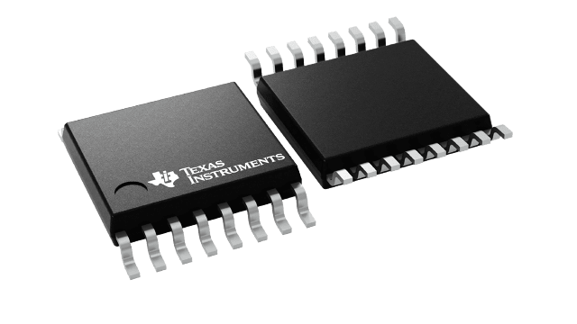
TLV5614IPWR
Active12-BIT, 3 US QUAD DAC, SERIAL INPUT, PGRMABLE SETTLING TIME, LOW POWER, H/W OR S/W POWERDOWN 16-TSSOP -40 TO 85
Deep-Dive with AI
Search across all available documentation for this part.
TLV5614IPWR
Active12-BIT, 3 US QUAD DAC, SERIAL INPUT, PGRMABLE SETTLING TIME, LOW POWER, H/W OR S/W POWERDOWN 16-TSSOP -40 TO 85
Technical Specifications
Parameters and characteristics commom to parts in this series
| Specification | TLV5614IPWR | TLV5614 Series |
|---|---|---|
| Architecture | String DAC | String DAC |
| Data Interface | SPI | SPI, QSPI™, DSP, MICROWIRE™, SPI™ |
| Differential Output | False | False |
| INL/DNL (LSB) [Max] | 1.5 LSB | 1.5 LSB |
| INL/DNL (LSB) [Min] | -1.5 LSB | -1.5 LSB |
| Mounting Type | Surface Mount | Surface Mount |
| Number of Bits | 12 | 12 |
| Number of D/A Converters | 4 | 4 |
| Operating Temperature [Max] | 85 °C | 70 - 125 ░C |
| Operating Temperature [Min] | -40 °C | -55 - 0 °C |
| Output Type | Voltage - Buffered | Voltage - Buffered |
| Package / Case | 16-TSSOP | 16-TSSOP, 16-SOIC |
| Package / Case | - | 0.154 - 3.9 mm Width |
| Package / Case [x] | 0.173 " | 0.173 " |
| Package / Case [x] | 4.4 mm | 4.4 mm |
| Reference Type | External | External |
| Settling Time | 20 µs | 9 - 20 µs |
| Supplier Device Package | 16-TSSOP | 16-TSSOP, 16-SOIC |
| Voltage - Supply, Analog | 5 V | 5 V |
| Voltage - Supply, Analog [Max] | 3.3 V | 3.3 V |
| Voltage - Supply, Analog [Min] | 2.7 V | 2.7 V |
| Voltage - Supply, Digital | 5 V | 5 V |
| Voltage - Supply, Digital [Max] | 3.3 V | 3.3 V |
| Voltage - Supply, Digital [Min] | 2.7 V | 2.7 V |
Pricing
Prices provided here are for design reference only. For realtime values and availability, please visit the distributors directly
TLV5614 Series
12-Bit, 3 us Quad DAC, Serial Input, Pgrmable Settling Time, Low Power, H/W or S/W PowerDown
| Part | Data Interface | Mounting Type | Voltage - Supply, Digital | Voltage - Supply, Digital [Min] | Voltage - Supply, Digital [Max] | Supplier Device Package | Differential Output | INL/DNL (LSB) [Max] | INL/DNL (LSB) [Min] | Package / Case [x] | Package / Case | Package / Case [x] | Operating Temperature [Max] | Operating Temperature [Min] | Output Type | Settling Time | Voltage - Supply, Analog [Max] | Voltage - Supply, Analog | Voltage - Supply, Analog [Min] | Number of Bits | Number of D/A Converters | Reference Type | Architecture | Package / Case |
|---|---|---|---|---|---|---|---|---|---|---|---|---|---|---|---|---|---|---|---|---|---|---|---|---|
Texas Instruments TLV5614CPWThe TLV5614 is a quadruple 12-bit voltage output digital-to-analog converter (DAC) with a flexible 4-wire serial interface. The 4-wire serial interface allows glueless interface to TMS320, SPI, QSPI, and Microwire serial ports. The TLV5614 is programmed with a 16-bit serial word comprised of a DAC address, individual DAC control bits, and a 12-bit DAC value. The device has provision for two supplies: one digital supply for the serial interface (via pins DVDDand DGND), and one for the DACs, reference buffers, and output buffers (via pins AVDDand AGND). Each supply is independent of the other, and can be any value between 2.7 V and 5.5 V. The dual supplies allow a typical application where the DAC will be controlled via a microprocessor operating on a 3 V supply (also used on pins DVDDand DGND), with the DACs operating on a 5 V supply. Of course, the digital and analog supplies can be tied together.
The resistor string output voltage is buffered by a x2 gain rail-to-rail output buffer. The buffer features a Class AB output stage to improve stability and reduce settling time. A rail-to-rail output stage and a power-down mode makes it ideal for single voltage, battery based applications. The settling time of the DAC is programmable to allow the designer to optimize speed versus power dissipation. The settling time is chosen by the control bits within the 16-bit serial input string. A high-impedance buffer is integrated on the REFINAB and REFINCD terminals to reduce the need for a low source impedance drive to the terminal. REFINAB and REFINCD allow DACs A and B to have a different reference voltage then DACs C and D.
The TLV5614 is implemented with a CMOS process and is available in a 16-terminal SOIC package. The TLV5614C is characterized for operation from 0°C to 70°C. The TLV5614I is characterized for operation from –40°C to 85°C.
The TLV5614 is a quadruple 12-bit voltage output digital-to-analog converter (DAC) with a flexible 4-wire serial interface. The 4-wire serial interface allows glueless interface to TMS320, SPI, QSPI, and Microwire serial ports. The TLV5614 is programmed with a 16-bit serial word comprised of a DAC address, individual DAC control bits, and a 12-bit DAC value. The device has provision for two supplies: one digital supply for the serial interface (via pins DVDDand DGND), and one for the DACs, reference buffers, and output buffers (via pins AVDDand AGND). Each supply is independent of the other, and can be any value between 2.7 V and 5.5 V. The dual supplies allow a typical application where the DAC will be controlled via a microprocessor operating on a 3 V supply (also used on pins DVDDand DGND), with the DACs operating on a 5 V supply. Of course, the digital and analog supplies can be tied together.
The resistor string output voltage is buffered by a x2 gain rail-to-rail output buffer. The buffer features a Class AB output stage to improve stability and reduce settling time. A rail-to-rail output stage and a power-down mode makes it ideal for single voltage, battery based applications. The settling time of the DAC is programmable to allow the designer to optimize speed versus power dissipation. The settling time is chosen by the control bits within the 16-bit serial input string. A high-impedance buffer is integrated on the REFINAB and REFINCD terminals to reduce the need for a low source impedance drive to the terminal. REFINAB and REFINCD allow DACs A and B to have a different reference voltage then DACs C and D.
The TLV5614 is implemented with a CMOS process and is available in a 16-terminal SOIC package. The TLV5614C is characterized for operation from 0°C to 70°C. The TLV5614I is characterized for operation from –40°C to 85°C. | SPI | Surface Mount | 5 V | 2.7 V | 3.3 V | 16-TSSOP | 1.5 LSB | -1.5 LSB | 0.173 " | 16-TSSOP | 4.4 mm | 70 ░C | 0 °C | Voltage - Buffered | 20 µs | 3.3 V | 5 V | 2.7 V | 12 | 4 | External | String DAC | ||
Texas Instruments TLV5614IDRThe TLV5614 is a quadruple 12-bit voltage output digital-to-analog converter (DAC) with a flexible 4-wire serial interface. The 4-wire serial interface allows glueless interface to TMS320, SPI, QSPI, and Microwire serial ports. The TLV5614 is programmed with a 16-bit serial word comprised of a DAC address, individual DAC control bits, and a 12-bit DAC value. The device has provision for two supplies: one digital supply for the serial interface (via pins DVDDand DGND), and one for the DACs, reference buffers, and output buffers (via pins AVDDand AGND). Each supply is independent of the other, and can be any value between 2.7 V and 5.5 V. The dual supplies allow a typical application where the DAC will be controlled via a microprocessor operating on a 3 V supply (also used on pins DVDDand DGND), with the DACs operating on a 5 V supply. Of course, the digital and analog supplies can be tied together.
The resistor string output voltage is buffered by a x2 gain rail-to-rail output buffer. The buffer features a Class AB output stage to improve stability and reduce settling time. A rail-to-rail output stage and a power-down mode makes it ideal for single voltage, battery based applications. The settling time of the DAC is programmable to allow the designer to optimize speed versus power dissipation. The settling time is chosen by the control bits within the 16-bit serial input string. A high-impedance buffer is integrated on the REFINAB and REFINCD terminals to reduce the need for a low source impedance drive to the terminal. REFINAB and REFINCD allow DACs A and B to have a different reference voltage then DACs C and D.
The TLV5614 is implemented with a CMOS process and is available in a 16-terminal SOIC package. The TLV5614C is characterized for operation from 0°C to 70°C. The TLV5614I is characterized for operation from –40°C to 85°C.
The TLV5614 is a quadruple 12-bit voltage output digital-to-analog converter (DAC) with a flexible 4-wire serial interface. The 4-wire serial interface allows glueless interface to TMS320, SPI, QSPI, and Microwire serial ports. The TLV5614 is programmed with a 16-bit serial word comprised of a DAC address, individual DAC control bits, and a 12-bit DAC value. The device has provision for two supplies: one digital supply for the serial interface (via pins DVDDand DGND), and one for the DACs, reference buffers, and output buffers (via pins AVDDand AGND). Each supply is independent of the other, and can be any value between 2.7 V and 5.5 V. The dual supplies allow a typical application where the DAC will be controlled via a microprocessor operating on a 3 V supply (also used on pins DVDDand DGND), with the DACs operating on a 5 V supply. Of course, the digital and analog supplies can be tied together.
The resistor string output voltage is buffered by a x2 gain rail-to-rail output buffer. The buffer features a Class AB output stage to improve stability and reduce settling time. A rail-to-rail output stage and a power-down mode makes it ideal for single voltage, battery based applications. The settling time of the DAC is programmable to allow the designer to optimize speed versus power dissipation. The settling time is chosen by the control bits within the 16-bit serial input string. A high-impedance buffer is integrated on the REFINAB and REFINCD terminals to reduce the need for a low source impedance drive to the terminal. REFINAB and REFINCD allow DACs A and B to have a different reference voltage then DACs C and D.
The TLV5614 is implemented with a CMOS process and is available in a 16-terminal SOIC package. The TLV5614C is characterized for operation from 0°C to 70°C. The TLV5614I is characterized for operation from –40°C to 85°C. | SPI | Surface Mount | 5 V | 2.7 V | 3.3 V | 16-SOIC | 1.5 LSB | -1.5 LSB | 16-SOIC | 85 °C | -40 °C | Voltage - Buffered | 20 µs | 3.3 V | 5 V | 2.7 V | 12 | 4 | External | String DAC | 0.154 in, 3.9 mm Width | |||
Texas Instruments TLV5614IPWThe TLV5614 is a quadruple 12-bit voltage output digital-to-analog converter (DAC) with a flexible 4-wire serial interface. The 4-wire serial interface allows glueless interface to TMS320, SPI, QSPI, and Microwire serial ports. The TLV5614 is programmed with a 16-bit serial word comprised of a DAC address, individual DAC control bits, and a 12-bit DAC value. The device has provision for two supplies: one digital supply for the serial interface (via pins DVDDand DGND), and one for the DACs, reference buffers, and output buffers (via pins AVDDand AGND). Each supply is independent of the other, and can be any value between 2.7 V and 5.5 V. The dual supplies allow a typical application where the DAC will be controlled via a microprocessor operating on a 3 V supply (also used on pins DVDDand DGND), with the DACs operating on a 5 V supply. Of course, the digital and analog supplies can be tied together.
The resistor string output voltage is buffered by a x2 gain rail-to-rail output buffer. The buffer features a Class AB output stage to improve stability and reduce settling time. A rail-to-rail output stage and a power-down mode makes it ideal for single voltage, battery based applications. The settling time of the DAC is programmable to allow the designer to optimize speed versus power dissipation. The settling time is chosen by the control bits within the 16-bit serial input string. A high-impedance buffer is integrated on the REFINAB and REFINCD terminals to reduce the need for a low source impedance drive to the terminal. REFINAB and REFINCD allow DACs A and B to have a different reference voltage then DACs C and D.
The TLV5614 is implemented with a CMOS process and is available in a 16-terminal SOIC package. The TLV5614C is characterized for operation from 0°C to 70°C. The TLV5614I is characterized for operation from –40°C to 85°C.
The TLV5614 is a quadruple 12-bit voltage output digital-to-analog converter (DAC) with a flexible 4-wire serial interface. The 4-wire serial interface allows glueless interface to TMS320, SPI, QSPI, and Microwire serial ports. The TLV5614 is programmed with a 16-bit serial word comprised of a DAC address, individual DAC control bits, and a 12-bit DAC value. The device has provision for two supplies: one digital supply for the serial interface (via pins DVDDand DGND), and one for the DACs, reference buffers, and output buffers (via pins AVDDand AGND). Each supply is independent of the other, and can be any value between 2.7 V and 5.5 V. The dual supplies allow a typical application where the DAC will be controlled via a microprocessor operating on a 3 V supply (also used on pins DVDDand DGND), with the DACs operating on a 5 V supply. Of course, the digital and analog supplies can be tied together.
The resistor string output voltage is buffered by a x2 gain rail-to-rail output buffer. The buffer features a Class AB output stage to improve stability and reduce settling time. A rail-to-rail output stage and a power-down mode makes it ideal for single voltage, battery based applications. The settling time of the DAC is programmable to allow the designer to optimize speed versus power dissipation. The settling time is chosen by the control bits within the 16-bit serial input string. A high-impedance buffer is integrated on the REFINAB and REFINCD terminals to reduce the need for a low source impedance drive to the terminal. REFINAB and REFINCD allow DACs A and B to have a different reference voltage then DACs C and D.
The TLV5614 is implemented with a CMOS process and is available in a 16-terminal SOIC package. The TLV5614C is characterized for operation from 0°C to 70°C. The TLV5614I is characterized for operation from –40°C to 85°C. | SPI | Surface Mount | 5 V | 2.7 V | 3.3 V | 16-TSSOP | 1.5 LSB | -1.5 LSB | 0.173 " | 16-TSSOP | 4.4 mm | 85 °C | -40 °C | Voltage - Buffered | 20 µs | 3.3 V | 5 V | 2.7 V | 12 | 4 | External | String DAC | ||
Texas Instruments TLV5614IPWRThe TLV5614 is a quadruple 12-bit voltage output digital-to-analog converter (DAC) with a flexible 4-wire serial interface. The 4-wire serial interface allows glueless interface to TMS320, SPI, QSPI, and Microwire serial ports. The TLV5614 is programmed with a 16-bit serial word comprised of a DAC address, individual DAC control bits, and a 12-bit DAC value. The device has provision for two supplies: one digital supply for the serial interface (via pins DVDDand DGND), and one for the DACs, reference buffers, and output buffers (via pins AVDDand AGND). Each supply is independent of the other, and can be any value between 2.7 V and 5.5 V. The dual supplies allow a typical application where the DAC will be controlled via a microprocessor operating on a 3 V supply (also used on pins DVDDand DGND), with the DACs operating on a 5 V supply. Of course, the digital and analog supplies can be tied together.
The resistor string output voltage is buffered by a x2 gain rail-to-rail output buffer. The buffer features a Class AB output stage to improve stability and reduce settling time. A rail-to-rail output stage and a power-down mode makes it ideal for single voltage, battery based applications. The settling time of the DAC is programmable to allow the designer to optimize speed versus power dissipation. The settling time is chosen by the control bits within the 16-bit serial input string. A high-impedance buffer is integrated on the REFINAB and REFINCD terminals to reduce the need for a low source impedance drive to the terminal. REFINAB and REFINCD allow DACs A and B to have a different reference voltage then DACs C and D.
The TLV5614 is implemented with a CMOS process and is available in a 16-terminal SOIC package. The TLV5614C is characterized for operation from 0°C to 70°C. The TLV5614I is characterized for operation from –40°C to 85°C.
The TLV5614 is a quadruple 12-bit voltage output digital-to-analog converter (DAC) with a flexible 4-wire serial interface. The 4-wire serial interface allows glueless interface to TMS320, SPI, QSPI, and Microwire serial ports. The TLV5614 is programmed with a 16-bit serial word comprised of a DAC address, individual DAC control bits, and a 12-bit DAC value. The device has provision for two supplies: one digital supply for the serial interface (via pins DVDDand DGND), and one for the DACs, reference buffers, and output buffers (via pins AVDDand AGND). Each supply is independent of the other, and can be any value between 2.7 V and 5.5 V. The dual supplies allow a typical application where the DAC will be controlled via a microprocessor operating on a 3 V supply (also used on pins DVDDand DGND), with the DACs operating on a 5 V supply. Of course, the digital and analog supplies can be tied together.
The resistor string output voltage is buffered by a x2 gain rail-to-rail output buffer. The buffer features a Class AB output stage to improve stability and reduce settling time. A rail-to-rail output stage and a power-down mode makes it ideal for single voltage, battery based applications. The settling time of the DAC is programmable to allow the designer to optimize speed versus power dissipation. The settling time is chosen by the control bits within the 16-bit serial input string. A high-impedance buffer is integrated on the REFINAB and REFINCD terminals to reduce the need for a low source impedance drive to the terminal. REFINAB and REFINCD allow DACs A and B to have a different reference voltage then DACs C and D.
The TLV5614 is implemented with a CMOS process and is available in a 16-terminal SOIC package. The TLV5614C is characterized for operation from 0°C to 70°C. The TLV5614I is characterized for operation from –40°C to 85°C. | SPI | Surface Mount | 5 V | 2.7 V | 3.3 V | 16-TSSOP | 1.5 LSB | -1.5 LSB | 0.173 " | 16-TSSOP | 4.4 mm | 85 °C | -40 °C | Voltage - Buffered | 20 µs | 3.3 V | 5 V | 2.7 V | 12 | 4 | External | String DAC | ||
Texas Instruments TLV5614CDThe TLV5614 is a quadruple 12-bit voltage output digital-to-analog converter (DAC) with a flexible 4-wire serial interface. The 4-wire serial interface allows glueless interface to TMS320, SPI, QSPI, and Microwire serial ports. The TLV5614 is programmed with a 16-bit serial word comprised of a DAC address, individual DAC control bits, and a 12-bit DAC value. The device has provision for two supplies: one digital supply for the serial interface (via pins DVDDand DGND), and one for the DACs, reference buffers, and output buffers (via pins AVDDand AGND). Each supply is independent of the other, and can be any value between 2.7 V and 5.5 V. The dual supplies allow a typical application where the DAC will be controlled via a microprocessor operating on a 3 V supply (also used on pins DVDDand DGND), with the DACs operating on a 5 V supply. Of course, the digital and analog supplies can be tied together.
The resistor string output voltage is buffered by a x2 gain rail-to-rail output buffer. The buffer features a Class AB output stage to improve stability and reduce settling time. A rail-to-rail output stage and a power-down mode makes it ideal for single voltage, battery based applications. The settling time of the DAC is programmable to allow the designer to optimize speed versus power dissipation. The settling time is chosen by the control bits within the 16-bit serial input string. A high-impedance buffer is integrated on the REFINAB and REFINCD terminals to reduce the need for a low source impedance drive to the terminal. REFINAB and REFINCD allow DACs A and B to have a different reference voltage then DACs C and D.
The TLV5614 is implemented with a CMOS process and is available in a 16-terminal SOIC package. The TLV5614C is characterized for operation from 0°C to 70°C. The TLV5614I is characterized for operation from –40°C to 85°C.
The TLV5614 is a quadruple 12-bit voltage output digital-to-analog converter (DAC) with a flexible 4-wire serial interface. The 4-wire serial interface allows glueless interface to TMS320, SPI, QSPI, and Microwire serial ports. The TLV5614 is programmed with a 16-bit serial word comprised of a DAC address, individual DAC control bits, and a 12-bit DAC value. The device has provision for two supplies: one digital supply for the serial interface (via pins DVDDand DGND), and one for the DACs, reference buffers, and output buffers (via pins AVDDand AGND). Each supply is independent of the other, and can be any value between 2.7 V and 5.5 V. The dual supplies allow a typical application where the DAC will be controlled via a microprocessor operating on a 3 V supply (also used on pins DVDDand DGND), with the DACs operating on a 5 V supply. Of course, the digital and analog supplies can be tied together.
The resistor string output voltage is buffered by a x2 gain rail-to-rail output buffer. The buffer features a Class AB output stage to improve stability and reduce settling time. A rail-to-rail output stage and a power-down mode makes it ideal for single voltage, battery based applications. The settling time of the DAC is programmable to allow the designer to optimize speed versus power dissipation. The settling time is chosen by the control bits within the 16-bit serial input string. A high-impedance buffer is integrated on the REFINAB and REFINCD terminals to reduce the need for a low source impedance drive to the terminal. REFINAB and REFINCD allow DACs A and B to have a different reference voltage then DACs C and D.
The TLV5614 is implemented with a CMOS process and is available in a 16-terminal SOIC package. The TLV5614C is characterized for operation from 0°C to 70°C. The TLV5614I is characterized for operation from –40°C to 85°C. | SPI | Surface Mount | 5 V | 2.7 V | 3.3 V | 16-SOIC | 1.5 LSB | -1.5 LSB | 16-SOIC | 70 ░C | 0 °C | Voltage - Buffered | 20 µs | 3.3 V | 5 V | 2.7 V | 12 | 4 | External | String DAC | 0.154 in, 3.9 mm Width | |||
SPI | Surface Mount | 5 V | 2.7 V | 3.3 V | 16-TSSOP | 1.5 LSB | -1.5 LSB | 0.173 " | 16-TSSOP | 4.4 mm | 70 ░C | 0 °C | Voltage - Buffered | 20 µs | 3.3 V | 5 V | 2.7 V | 12 | 4 | External | String DAC | |||
Texas Instruments TLV5614MPWREPThe TLV5614 is a quadruple 12-bit voltage output digital-to-analog converter (DAC) with a flexible four-wire serial interface. The four-wire serial interface allows glueless interface to TMS320™ DSP family, SPI™, QSPI™, and Microwire™ serial ports. The TLV5614 is programmed with a 16-bit serial word comprised of a DAC address, individual DAC control bits, and a 12-bit DAC value. The device has provision for two supplies - one digital supply for the serial interface (via pins DVDDand DGND), and one for the DACs, reference buffers, and output buffers (via pins AVDD and AGND). Each supply is independent of the other and can be any value between 2.7 V and 5.5 V. The dual supplies allow a typical application where the DAC is controlled via a microprocessor operating on a 3-V supply (also used on pins DVDDand DGND), with the DACs operating on a 5-V supply. The digital and analog supplies can be tied together.
The resistor string output voltage is buffered by a 2× gain rail-to-rail output buffer. The buffer features a Class AB output stage to improve stability and reduce settling time. A rail-to-rail output stage and a power-down mode makes it ideal for single-voltage, battery-based applications. The settling time of the DAC is programmable to allow the designer to optimize speed versus power dissipation. The settling time is chosen by the control bits within the 16-bit serial input string. A high-impedance buffer is integrated on the REFINAB and REFINCD terminals to reduce the need for a low source-impedance drive to the terminal. REFINAB and REFINCD allow DAC A and B to have a different reference voltage than DAC C and D.
The TLV5614 is implemented with a CMOS process and is available in a 16-terminal TSSOP package. The TLV5614M is characterized for operation from -55°C to 125°C.
The TLV5614 is a quadruple 12-bit voltage output digital-to-analog converter (DAC) with a flexible four-wire serial interface. The four-wire serial interface allows glueless interface to TMS320™ DSP family, SPI™, QSPI™, and Microwire™ serial ports. The TLV5614 is programmed with a 16-bit serial word comprised of a DAC address, individual DAC control bits, and a 12-bit DAC value. The device has provision for two supplies - one digital supply for the serial interface (via pins DVDDand DGND), and one for the DACs, reference buffers, and output buffers (via pins AVDD and AGND). Each supply is independent of the other and can be any value between 2.7 V and 5.5 V. The dual supplies allow a typical application where the DAC is controlled via a microprocessor operating on a 3-V supply (also used on pins DVDDand DGND), with the DACs operating on a 5-V supply. The digital and analog supplies can be tied together.
The resistor string output voltage is buffered by a 2× gain rail-to-rail output buffer. The buffer features a Class AB output stage to improve stability and reduce settling time. A rail-to-rail output stage and a power-down mode makes it ideal for single-voltage, battery-based applications. The settling time of the DAC is programmable to allow the designer to optimize speed versus power dissipation. The settling time is chosen by the control bits within the 16-bit serial input string. A high-impedance buffer is integrated on the REFINAB and REFINCD terminals to reduce the need for a low source-impedance drive to the terminal. REFINAB and REFINCD allow DAC A and B to have a different reference voltage than DAC C and D.
The TLV5614 is implemented with a CMOS process and is available in a 16-terminal TSSOP package. The TLV5614M is characterized for operation from -55°C to 125°C. | DSP, MICROWIRE™, QSPI™, SPI™ | Surface Mount | 5 V | 2.7 V | 3.3 V | 16-TSSOP | 1.5 LSB | -1.5 LSB | 0.173 " | 16-TSSOP | 4.4 mm | 125 °C | -55 °C | Voltage - Buffered | 9 µs | 3.3 V | 5 V | 2.7 V | 12 | 4 | External | String DAC | ||
Texas Instruments TLV5614CPWRThe TLV5614 is a quadruple 12-bit voltage output digital-to-analog converter (DAC) with a flexible 4-wire serial interface. The 4-wire serial interface allows glueless interface to TMS320, SPI, QSPI, and Microwire serial ports. The TLV5614 is programmed with a 16-bit serial word comprised of a DAC address, individual DAC control bits, and a 12-bit DAC value. The device has provision for two supplies: one digital supply for the serial interface (via pins DVDDand DGND), and one for the DACs, reference buffers, and output buffers (via pins AVDDand AGND). Each supply is independent of the other, and can be any value between 2.7 V and 5.5 V. The dual supplies allow a typical application where the DAC will be controlled via a microprocessor operating on a 3 V supply (also used on pins DVDDand DGND), with the DACs operating on a 5 V supply. Of course, the digital and analog supplies can be tied together.
The resistor string output voltage is buffered by a x2 gain rail-to-rail output buffer. The buffer features a Class AB output stage to improve stability and reduce settling time. A rail-to-rail output stage and a power-down mode makes it ideal for single voltage, battery based applications. The settling time of the DAC is programmable to allow the designer to optimize speed versus power dissipation. The settling time is chosen by the control bits within the 16-bit serial input string. A high-impedance buffer is integrated on the REFINAB and REFINCD terminals to reduce the need for a low source impedance drive to the terminal. REFINAB and REFINCD allow DACs A and B to have a different reference voltage then DACs C and D.
The TLV5614 is implemented with a CMOS process and is available in a 16-terminal SOIC package. The TLV5614C is characterized for operation from 0°C to 70°C. The TLV5614I is characterized for operation from –40°C to 85°C.
The TLV5614 is a quadruple 12-bit voltage output digital-to-analog converter (DAC) with a flexible 4-wire serial interface. The 4-wire serial interface allows glueless interface to TMS320, SPI, QSPI, and Microwire serial ports. The TLV5614 is programmed with a 16-bit serial word comprised of a DAC address, individual DAC control bits, and a 12-bit DAC value. The device has provision for two supplies: one digital supply for the serial interface (via pins DVDDand DGND), and one for the DACs, reference buffers, and output buffers (via pins AVDDand AGND). Each supply is independent of the other, and can be any value between 2.7 V and 5.5 V. The dual supplies allow a typical application where the DAC will be controlled via a microprocessor operating on a 3 V supply (also used on pins DVDDand DGND), with the DACs operating on a 5 V supply. Of course, the digital and analog supplies can be tied together.
The resistor string output voltage is buffered by a x2 gain rail-to-rail output buffer. The buffer features a Class AB output stage to improve stability and reduce settling time. A rail-to-rail output stage and a power-down mode makes it ideal for single voltage, battery based applications. The settling time of the DAC is programmable to allow the designer to optimize speed versus power dissipation. The settling time is chosen by the control bits within the 16-bit serial input string. A high-impedance buffer is integrated on the REFINAB and REFINCD terminals to reduce the need for a low source impedance drive to the terminal. REFINAB and REFINCD allow DACs A and B to have a different reference voltage then DACs C and D.
The TLV5614 is implemented with a CMOS process and is available in a 16-terminal SOIC package. The TLV5614C is characterized for operation from 0°C to 70°C. The TLV5614I is characterized for operation from –40°C to 85°C. | SPI | Surface Mount | 5 V | 2.7 V | 3.3 V | 16-TSSOP | 1.5 LSB | -1.5 LSB | 0.173 " | 16-TSSOP | 4.4 mm | 70 ░C | 0 °C | Voltage - Buffered | 20 µs | 3.3 V | 5 V | 2.7 V | 12 | 4 | External | String DAC | ||
Texas Instruments TLV5614IDThe TLV5614 is a quadruple 12-bit voltage output digital-to-analog converter (DAC) with a flexible 4-wire serial interface. The 4-wire serial interface allows glueless interface to TMS320, SPI, QSPI, and Microwire serial ports. The TLV5614 is programmed with a 16-bit serial word comprised of a DAC address, individual DAC control bits, and a 12-bit DAC value. The device has provision for two supplies: one digital supply for the serial interface (via pins DVDDand DGND), and one for the DACs, reference buffers, and output buffers (via pins AVDDand AGND). Each supply is independent of the other, and can be any value between 2.7 V and 5.5 V. The dual supplies allow a typical application where the DAC will be controlled via a microprocessor operating on a 3 V supply (also used on pins DVDDand DGND), with the DACs operating on a 5 V supply. Of course, the digital and analog supplies can be tied together.
The resistor string output voltage is buffered by a x2 gain rail-to-rail output buffer. The buffer features a Class AB output stage to improve stability and reduce settling time. A rail-to-rail output stage and a power-down mode makes it ideal for single voltage, battery based applications. The settling time of the DAC is programmable to allow the designer to optimize speed versus power dissipation. The settling time is chosen by the control bits within the 16-bit serial input string. A high-impedance buffer is integrated on the REFINAB and REFINCD terminals to reduce the need for a low source impedance drive to the terminal. REFINAB and REFINCD allow DACs A and B to have a different reference voltage then DACs C and D.
The TLV5614 is implemented with a CMOS process and is available in a 16-terminal SOIC package. The TLV5614C is characterized for operation from 0°C to 70°C. The TLV5614I is characterized for operation from –40°C to 85°C.
The TLV5614 is a quadruple 12-bit voltage output digital-to-analog converter (DAC) with a flexible 4-wire serial interface. The 4-wire serial interface allows glueless interface to TMS320, SPI, QSPI, and Microwire serial ports. The TLV5614 is programmed with a 16-bit serial word comprised of a DAC address, individual DAC control bits, and a 12-bit DAC value. The device has provision for two supplies: one digital supply for the serial interface (via pins DVDDand DGND), and one for the DACs, reference buffers, and output buffers (via pins AVDDand AGND). Each supply is independent of the other, and can be any value between 2.7 V and 5.5 V. The dual supplies allow a typical application where the DAC will be controlled via a microprocessor operating on a 3 V supply (also used on pins DVDDand DGND), with the DACs operating on a 5 V supply. Of course, the digital and analog supplies can be tied together.
The resistor string output voltage is buffered by a x2 gain rail-to-rail output buffer. The buffer features a Class AB output stage to improve stability and reduce settling time. A rail-to-rail output stage and a power-down mode makes it ideal for single voltage, battery based applications. The settling time of the DAC is programmable to allow the designer to optimize speed versus power dissipation. The settling time is chosen by the control bits within the 16-bit serial input string. A high-impedance buffer is integrated on the REFINAB and REFINCD terminals to reduce the need for a low source impedance drive to the terminal. REFINAB and REFINCD allow DACs A and B to have a different reference voltage then DACs C and D.
The TLV5614 is implemented with a CMOS process and is available in a 16-terminal SOIC package. The TLV5614C is characterized for operation from 0°C to 70°C. The TLV5614I is characterized for operation from –40°C to 85°C. | SPI | Surface Mount | 5 V | 2.7 V | 3.3 V | 16-SOIC | 1.5 LSB | -1.5 LSB | 16-SOIC | 85 °C | -40 °C | Voltage - Buffered | 20 µs | 3.3 V | 5 V | 2.7 V | 12 | 4 | External | String DAC | 0.154 in, 3.9 mm Width |
Description
General part information
TLV5614 Series
The TLV5614 is a quadruple 12-bit voltage output digital-to-analog converter (DAC) with a flexible 4-wire serial interface. The 4-wire serial interface allows glueless interface to TMS320, SPI, QSPI, and Microwire serial ports. The TLV5614 is programmed with a 16-bit serial word comprised of a DAC address, individual DAC control bits, and a 12-bit DAC value. The device has provision for two supplies: one digital supply for the serial interface (via pins DVDDand DGND), and one for the DACs, reference buffers, and output buffers (via pins AVDDand AGND). Each supply is independent of the other, and can be any value between 2.7 V and 5.5 V. The dual supplies allow a typical application where the DAC will be controlled via a microprocessor operating on a 3 V supply (also used on pins DVDDand DGND), with the DACs operating on a 5 V supply. Of course, the digital and analog supplies can be tied together.
The resistor string output voltage is buffered by a x2 gain rail-to-rail output buffer. The buffer features a Class AB output stage to improve stability and reduce settling time. A rail-to-rail output stage and a power-down mode makes it ideal for single voltage, battery based applications. The settling time of the DAC is programmable to allow the designer to optimize speed versus power dissipation. The settling time is chosen by the control bits within the 16-bit serial input string. A high-impedance buffer is integrated on the REFINAB and REFINCD terminals to reduce the need for a low source impedance drive to the terminal. REFINAB and REFINCD allow DACs A and B to have a different reference voltage then DACs C and D.
The TLV5614 is implemented with a CMOS process and is available in a 16-terminal SOIC package. The TLV5614C is characterized for operation from 0°C to 70°C. The TLV5614I is characterized for operation from –40°C to 85°C.
Documents
Technical documentation and resources