CDCM61001RHBR/2801
ActiveIC CLOCK GENERATOR 32VQFN
CDCM61001RHBR/2801
ActiveIC CLOCK GENERATOR 32VQFN
Description
General part information
CDCM61001 Series
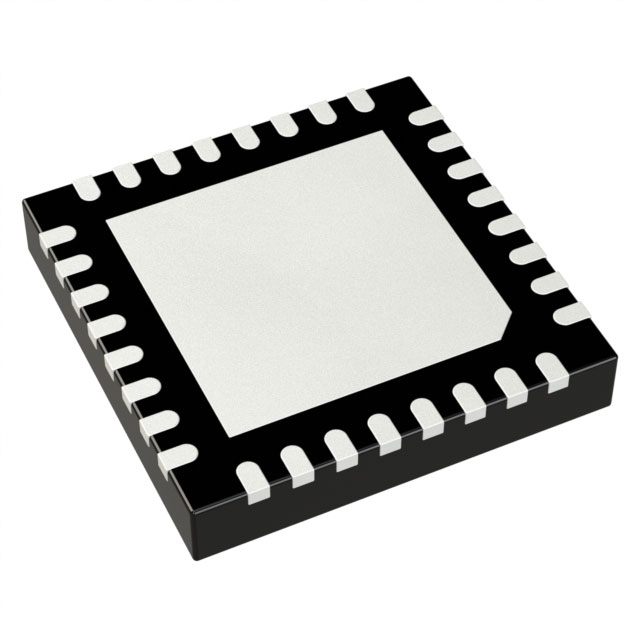
The CDCM61001 is a highly versatile, low-jitter frequency synthesizer that can generate low-jitter clock outputs, selectable between low-voltage positive emitter coupled logic (LVPECL), low-voltage differential signaling (LVDS), or low-voltage complementary metal oxide semiconductor (LVCMOS) outputs, from a low-frequency crystal or LVCMOS input for a variety of wireline and data communication applications. The CDCM61001 features an onboard PLL that can be easily configured solely through control pins. The overall output random jitter performance is less than 1ps, RMS (from 10 kHz to 20 MHz), making this device a perfect choice for use in demanding applications such as SONET, Ethernet, Fibre Channel, and SAN. The CDCM61001 is available in a small, 32-pin, 5-mm × 5-mm QFN package.
The CDCM61001 is a high-performance, low phase noise, fully-integrated voltage-controlled oscillator (VCO) clock synthesizer with one universal output buffer that can be configured to be LVPECL, LVDS, or LVCMOS compatible. The universal output can also be converted to two LVCMOS outputs. Additionally, an LVCMOS bypass output clock is available in an output configuration which can help with crystal loading in order to achieve an exact desired input frequency. It has one fully-integrated, low-noise, LC-based VCO that operates in the 1.75 GHz to 2.05 GHz range.
The phase-locked loop (PLL) synchronizes the VCO with respect to the input, which can either be a low-frequency crystal. The output has an output divider sourced from the VCO core. All device settings are managed through a control pin structure, which has two pins that control the prescaler and feedback divider, three pins that control the output divider, two pins that control the output type, and one pin that controls the output enable. Any time the PLL settings (including the input frequency, prescaler divider, or feedback divider) are altered, a reset must be issued through the Reset control pin (active low for device reset). The reset initiates a PLL recalibration process to ensure PLL lock. When the device is in reset, the outputs and divider are turned off.
Technical Specifications
Parameters and characteristics for this part
| Specification | CDCM61001RHBR/2801 |
|---|---|
| Differential Input | No |
| Differential Output | No |
| Divider | Yes |
| Frequency - Max | 683.28 MHz |
| Input | LVCMOS, Crystal |
| Input Ratio | 1 |
| Mounting Type | Surface Mount |
| Multiplier | No |
| Number of Circuits | 1 |
| Operating Temperature (Max) | 85 °C |
| Operating Temperature (Min) | -40 °C |
| Output | LVCMOS, LVPECL, LVDS |
| Output Ratio | 2 |
| Package / Case | 32-VFQFN Exposed Pad |
| Package Length | 5 mm |
| Package Name | 32-VQFN |
| Package Width | 5 mm |
| PLL | Yes with Bypass |
| Type | Clock Generator |
| Voltage - Supply (Maximum) | 3.6 V |
| Voltage - Supply (Minimum) | 3 V |
Pricing
Prices provided here are for design reference only. For realtime values and availability, please visit the distributors directly
Sign in to see pricing
Create a free account to access distributor pricing data.
CAD
3D models and CAD resources for this part
Documents
Technical documentation and resources
No documents available