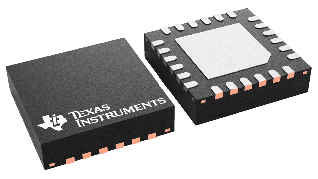
TPS51124RGER
Active3-V TO 28-V, DUAL-SYNCHRONOUS BUCK CONTROLLER FOR LOW OUTPUT VOLTAGE RAILS
TPS51124RGER
Active3-V TO 28-V, DUAL-SYNCHRONOUS BUCK CONTROLLER FOR LOW OUTPUT VOLTAGE RAILS
Description
General part information
TPS51124 Series
The TPS51124 is a dual, adaptive on-time D-CAP™ mode synchronous buck controller. The part enables system designers to cost effectively complete the suite of notebook power bus regulators with the absolute lowest external component count and lowest standby consumption. The fixed frequency emulated adaptive on-time control supports seamless operation between PWM mode at heavy load condition and reduced frequency operation at light load for high efficiency down to milliampere range. The main control loop for the TPS51124 uses the D-CAP mode that optimized for low ESR output capacitors such as POSCAP or SP-CAP promises fast transient response with no external compensation. Simple and separate power good signals for each channel allow flexibility of power sequencing. The part provides a convenient and efficient operation with supply input voltages (V5IN, V5FILT) ranging from 4.5 V to 5.5 V, conversion voltages (drain voltage for the synchronous high-side MOSFET) from 3 V to 28 V and output voltages from 0.76 V to 5.5 V.
The TPS51124 is available in 24-pin VQFN package specified from –40°C to 85°C ambient temperature range.
The TPS51124 is a dual, adaptive on-time D-CAP™ mode synchronous buck controller. The part enables system designers to cost effectively complete the suite of notebook power bus regulators with the absolute lowest external component count and lowest standby consumption. The fixed frequency emulated adaptive on-time control supports seamless operation between PWM mode at heavy load condition and reduced frequency operation at light load for high efficiency down to milliampere range. The main control loop for the TPS51124 uses the D-CAP mode that optimized for low ESR output capacitors such as POSCAP or SP-CAP promises fast transient response with no external compensation. Simple and separate power good signals for each channel allow flexibility of power sequencing. The part provides a convenient and efficient operation with supply input voltages (V5IN, V5FILT) ranging from 4.5 V to 5.5 V, conversion voltages (drain voltage for the synchronous high-side MOSFET) from 3 V to 28 V and output voltages from 0.76 V to 5.5 V.
Technical Specifications
Parameters and characteristics for this part
| Specification | TPS51124RGER |
|---|---|
| Clock Sync | No |
| Control Features | Enable, On Time Control, Power Good |
| Function | Step-Down |
| Mounting Type | Surface Mount |
| Number of Outputs | 2 |
| Operating Temperature (Max) | 85 °C |
| Operating Temperature (Min) | -40 °C |
| Output Configuration | Positive |
| Output Phases | 1 |
| Output Type | Transistor Driver |
| Package / Case | 24-VFQFN Exposed Pad |
| Package Length | 4 mm |
| Package Name | 24-VQFN |
| Package Width | 4 mm |
| Synchronous Rectifier | Yes |
| Topology | Buck |
| Voltage - Supply (Vcc/Vdd) Maximum | 5.5 V |
| Voltage - Supply (Vcc/Vdd) Minimum | 4.5 V |
Pricing
Prices provided here are for design reference only. For realtime values and availability, please visit the distributors directly
Sign in to see pricing
Create a free account to access distributor pricing data.
CAD
3D models and CAD resources for this part
Documents
Technical documentation and resources