ADS6225IRGZT
ActiveDUAL-CHANNEL, 12-BIT, 125-MSPS ANALOG-TO-DIGITAL CONVERTER (ADC)
ADS6225IRGZT
ActiveDUAL-CHANNEL, 12-BIT, 125-MSPS ANALOG-TO-DIGITAL CONVERTER (ADC)
Description
General part information
ADS6225 Series
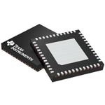
ADS6225/ADS6224/ADS6223/ADS6222 (ADS622X) is a family of high performance 12-bit 125/105/80/65 MSPS dual channel A-D converters. Serial LVDS data outputs reduce the number of interface lines, resulting in a compact 48-pin QFN package (7 mm × 7 mm) that allows for high system integration density. The device includes 3.5 dB coarse gain option that can be used to improve SFDR performance with little degradation in SNR. In addition to the coarse gain, fine gain options also exist, programmable in 1 dB steps up to 6 dB.
The output interface is 2-wire, where each ADC data is serialized and output over two LVDS pairs. This makes it possible to halve the serial data rate (compared to a 1-wire interface) and restrict it to less than 1 Gbps easing receiver design. The ADS622X also includes the traditional 1-wire interface that can be used at lower sampling frequencies.
An internal phase lock loop (PLL) multiplies the incoming ADC sampling clock to derive the bit clock. The bit clock is used to serialize the ADC data from each channel. In addition to the serial data streams, the frame and bit clocks are also transmitted as LVDS outputs. The LVDS output buffers have features such as programmable LVDS currents, current doubling modes and internal termination options. These can be used to widen eye-openings and improve signal integrity, easing capture by the receiver.
Technical Specifications
Parameters and characteristics for this part
| Specification | ADS6225IRGZT |
|---|---|
| Architecture | Pipelined |
| Configuration | S/H-ADC |
| Data Interface | LVDS - Serial |
| Features | Simultaneous Sampling |
| Input Type | Differential |
| Mounting Type | Surface Mount |
| Number of A/D Converters | 2 count |
| Number of Bits | 12 bits |
| Number of Inputs | 2 |
| Operating Temperature (Max) | 85 °C |
| Operating Temperature (Min) | -40 °C |
| Package / Case | 48-VFQFN Exposed Pad |
| Package Length | 7 mm |
| Package Name | 48-VQFN |
| Package Width | 7 mm |
| Ratio - ADC | 1 |
| Ratio - S/H | 1 |
| Reference Type | External, Internal |
| Sampling Rate (Per Second) | 125 MHz |
| Voltage - Supply, Analog (Max) | 3.6 V |
| Voltage - Supply, Analog (Min) | 3 V |
| Voltage - Supply, Digital (Max) | 3.6 V |
| Voltage - Supply, Digital (Min) | 3 V |
Pricing
Prices provided here are for design reference only. For realtime values and availability, please visit the distributors directly
Sign in to see pricing
Create a free account to access distributor pricing data.
CAD
3D models and CAD resources for this part
Documents
Technical documentation and resources