LMK00308SQE/NOPB
Active3.1-GHZ DIFFERENTIAL CLOCK BUFFER/LEVEL TRANSLATOR WITH 8 CONFIGURABLE OUTPUTS
LMK00308SQE/NOPB
Active3.1-GHZ DIFFERENTIAL CLOCK BUFFER/LEVEL TRANSLATOR WITH 8 CONFIGURABLE OUTPUTS
Description
General part information
LMK00308 Series
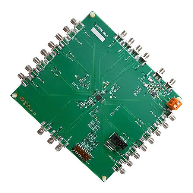
The LMK00308 is a 3-GHz, 8-output differential fanout buffer intended for high-frequency, low-jitter clock/data distribution and level translation. The input clock can be selected from two universal inputs or one crystal input. The selected input clock is distributed to two banks of 4 differential outputs and one LVCMOS output. Both differential output banks can be independently configured as LVPECL, LVDS, or HCSL drivers, or disabled. The LVCMOS output has a synchronous enable input for runt-pulse-free operation when enabled or disabled. The LMK00308 operates from a 3.3 V core supply and 3 independent 3.3 V/2.5 V output supplies.
The LMK00308 provides high performance, versatility, and power efficiency, making it ideal for replacing fixed-output buffer devices while increasing timing margin in the system.
The LMK00308 is a 3-GHz, 8-output differential fanout buffer intended for high-frequency, low-jitter clock/data distribution and level translation. The input clock can be selected from two universal inputs or one crystal input. The selected input clock is distributed to two banks of 4 differential outputs and one LVCMOS output. Both differential output banks can be independently configured as LVPECL, LVDS, or HCSL drivers, or disabled. The LVCMOS output has a synchronous enable input for runt-pulse-free operation when enabled or disabled. The LMK00308 operates from a 3.3 V core supply and 3 independent 3.3 V/2.5 V output supplies.
Technical Specifications
Parameters and characteristics for this part
| Specification | LMK00308SQE/NOPB |
|---|---|
| Differential Input | Yes |
| Differential Output | Yes |
| Frequency - Max | 3.1 GHz |
| Input | SSTL, LVPECL, CML, HCSL, Crystal, LVDS, HSTL |
| Input Ratio | 3 |
| Mounting Type | Surface Mount |
| Number of Circuits | 1 |
| Operating Temperature (Max) | 85 °C |
| Operating Temperature (Min) | -40 °C |
| Output | LVCMOS, LVPECL, LVDS, HCSL |
| Output Ratio | 9 |
| Package / Case | 40-WFQFN Exposed Pad |
| Package Length | 6 mm |
| Package Name | 40-WQFN |
| Package Width | 6 mm |
| Type | Fanout Buffer (Distribution), Multiplexer, Translator |
| Voltage - Supply (Maximum) | 3.45 V |
| Voltage - Supply (Minimum) | 3.15 V |
Pricing
Prices provided here are for design reference only. For realtime values and availability, please visit the distributors directly
Sign in to see pricing
Create a free account to access distributor pricing data.
CAD
3D models and CAD resources for this part