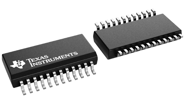
CDCF5801DBQR
ActiveLOW-JITTER PLL-BASED MULTIPLIER & DIVIDER WITH PROGRAMMABLE DELAY LINES DOWN TO SUB 10 PS
Deep-Dive with AI
Search across all available documentation for this part.

CDCF5801DBQR
ActiveLOW-JITTER PLL-BASED MULTIPLIER & DIVIDER WITH PROGRAMMABLE DELAY LINES DOWN TO SUB 10 PS
Deep-Dive with AI
Technical Specifications
Parameters and characteristics commom to parts in this series
| Specification | CDCF5801DBQR | CDCF5801 Series |
|---|---|---|
| Differential - Input:Output | No/Yes | No/Yes |
| Frequency - Max [Max] | 280 MHz | 280 MHz |
| Input | HSTL, LVPECL, LVTTL | HSTL, LVPECL, LVTTL |
| Mounting Type | Surface Mount | Surface Mount |
| Number of Circuits | 1 | 1 |
| Operating Temperature [Max] | 85 °C | 85 °C |
| Operating Temperature [Min] | -40 °C | -40 °C |
| Output | SSTL, LVPECL, HSTL, LVTTL, LVDS | SSTL, LVPECL, HSTL, LVTTL, LVDS |
| Package / Case | 24-SSOP | 24-SSOP |
| PLL | True | True |
| Ratio - Input:Output [custom] | 1:1 | 1:1 |
| Supplier Device Package | 24-SSOP | 24-SSOP |
| Type | PLL Multiplier/Divider | PLL Multiplier/Divider |
| Voltage - Supply [Max] | 3.6 V | 3.6 V |
| Voltage - Supply [Min] | 3 V | 3 V |
Pricing
Prices provided here are for design reference only. For realtime values and availability, please visit the distributors directly
| Distributor | Package | Quantity | $ | |
|---|---|---|---|---|
| Digikey | Tape & Reel (TR) | 2500 | $ 5.12 | |
| Texas Instruments | LARGE T&R | 1 | $ 8.25 | |
| 100 | $ 6.73 | |||
| 250 | $ 5.29 | |||
| 1000 | $ 4.49 | |||
CDCF5801 Series
Low-jitter PLL-based multiplier & divider with programmable delay lines down to sub 10 ps
| Part | Mounting Type | Voltage - Supply [Max] | Voltage - Supply [Min] | Operating Temperature [Min] | Operating Temperature [Max] | Number of Circuits | Package / Case | Frequency - Max [Max] | Output | Type | Supplier Device Package | Ratio - Input:Output [custom] | Differential - Input:Output | Input | PLL |
|---|---|---|---|---|---|---|---|---|---|---|---|---|---|---|---|
Texas Instruments CDCF5801ADBQR | Surface Mount | 3.6 V | 3 V | -40 °C | 85 °C | 1 | 24-SSOP | 280 MHz | HSTL, LVDS, LVPECL, LVTTL, SSTL | PLL Multiplier/Divider | 24-SSOP | 1:1 | No/Yes | HSTL, LVPECL, LVTTL | |
Texas Instruments CDCF5801ADBQ | Surface Mount | 3.6 V | 3 V | -40 °C | 85 °C | 1 | 24-SSOP | 280 MHz | HSTL, LVDS, LVPECL, LVTTL, SSTL | PLL Multiplier/Divider | 24-SSOP | 1:1 | No/Yes | HSTL, LVPECL, LVTTL | |
Texas Instruments CDCF5801DBQ | Surface Mount | 3.6 V | 3 V | -40 °C | 85 °C | 1 | 24-SSOP | 280 MHz | HSTL, LVDS, LVPECL, LVTTL, SSTL | PLL Multiplier/Divider | 24-SSOP | 1:1 | No/Yes | HSTL, LVPECL, LVTTL | |
Texas Instruments CDCF5801ADBQG4 | Surface Mount | 3.6 V | 3 V | -40 °C | 85 °C | 1 | 24-SSOP | 280 MHz | HSTL, LVDS, LVPECL, LVTTL, SSTL | PLL Multiplier/Divider | 24-SSOP | 1:1 | No/Yes | HSTL, LVPECL, LVTTL | |
Texas Instruments CDCF5801DBQR | Surface Mount | 3.6 V | 3 V | -40 °C | 85 °C | 1 | 24-SSOP | 280 MHz | HSTL, LVDS, LVPECL, LVTTL, SSTL | PLL Multiplier/Divider | 24-SSOP | 1:1 | No/Yes | HSTL, LVPECL, LVTTL |
Description
General part information
CDCF5801 Series
The CDCF5801A provides clock multiplication from a reference clock (REFCLK) signal with the unique capability to delay or advance the CLKOUT/CLKOUTB with steps of only 1.3 mUI through a phase aligner. For every rising edge on the DLYCTRL pin the CLKOUT is delayed by a 1.3-mUI step size as long as the LEADLAG input detects a low signal at the time of the DLYCTRL rising edge. Similarly for every rising edge on the DLYCTRL pin the CLKOUT is advanced by a 1.3-mUI step size as long as the LEADLAG pin is high during the transition. This unique capability allows the device to phase align (zero delay) between CLKOUT/CLKOUTB and any one other CLK in the system by feeding the clocks that need to be aligned to the DLYCTRL and the LEADLAG pins. Also it provides the capability to program a fixed delay by providing the proper number of edges on the DLYCTRL pin, while strapping the LEADLAG pin to dc high or low. Further possible applications are:
The CDCF5801A has a fail-safe power up initialization state-machine which supports proper operation under all power up conditions.
The CDCF5801A provides clock multiplication and division from a reference clock (REFCLK) signal. The device is optimized to have extremely low jitter impact from input to output. The predivider pins MULT[0:1] and post-divider pins P[0:2] provide selection for frequency multiplication and division ratios, generating CLKOUT/CLOUTKB frequencies ranging from 25 MHz to 280 MHz with clock input references (REFCLK) ranging from 12.5 MHz to 240 MHz. See for detailed frequency support. The selection of pins MULT[0:1] and P[1:2] determines the multiplication value of 1, 2, 4, or 8. The CDCF5801A offers several power-down/ high-impedance modes, selectable by pins P0, STOPB and PWRDN. Another unique capability of the CDCF5801A is the high sensitivity and wide common-mode range of the clock-input pin REFCLK by varying the voltage on the VDDREF pin. The clock signal outputs CLKOUT and CLKOUTB can be used independently to generate single-ended clock signals. The CLKOUT/CLKOUTB outputs can also be combined to generate a differential output signal suitable for LVDS, LVPECL, or HSTL/SSTL signaling. The CDCF5801A is characterized for operation over free-air temperatures of -40°C to 85°C.
Documents
Technical documentation and resources


