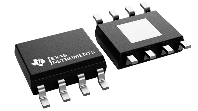
UCC27301AQDRCRQ1
ActiveAUTOMOTIVE 120V 4A HALF-BRIDGE DRIVER WITH 8V UVLO, ENABLE AND INTERLOCK
UCC27301AQDRCRQ1
ActiveAUTOMOTIVE 120V 4A HALF-BRIDGE DRIVER WITH 8V UVLO, ENABLE AND INTERLOCK
Description
General part information
UCC27301A-Q1 Series
The UCC27301A-Q1 is a robust gate driver designed to drive two N-channel MOSFETs in a half-bridge or synchronous buck configuration with an absolute maximum bootstrap voltage of 120V. Its 3.7A peak source and 4.5A peak sink current capability allows the UCC27301A-Q1 to drive large power MOSFETs with minimized switching losses during the transition through the Miller Plateau. The switching node (HS pin) can handle negative transient voltage, which allows the high-side channel to be protected from inherent negative voltages caused by parasitic inductance and stray capacitance.
The inputs are independent of supply voltage and are able to withstand -10V and +20V absolute maximum ratings. The low-side and high-side gate drivers are matched to 4ns between the turn on and turn off of each other and are controlled throught the LI and HI input pins respectively. However, the input interlock logic will turn both driver outputs low whenever both LI and HI inputs are high at the same time. An on-chip 120V rated bootstrap diode eliminates the need to add discrete bootstrap diodes. Undervoltage lockout (UVLO) is provided for both the high-side and the low-side drivers which provides symmetric turn on and turn off behavior and forces the outputs low if the drive voltage is below the specified threshold.
The UCC27301A-Q1 is a robust gate driver designed to drive two N-channel MOSFETs in a half-bridge or synchronous buck configuration with an absolute maximum bootstrap voltage of 120V. Its 3.7A peak source and 4.5A peak sink current capability allows the UCC27301A-Q1 to drive large power MOSFETs with minimized switching losses during the transition through the Miller Plateau. The switching node (HS pin) can handle negative transient voltage, which allows the high-side channel to be protected from inherent negative voltages caused by parasitic inductance and stray capacitance.
Technical Specifications
Parameters and characteristics for this part
| Specification | UCC27301AQDRCRQ1 |
|---|---|
| Channel Type | Independent |
| Current - Peak Output (Sink) | 3.7 A |
| Current - Peak Output (Source) | 4.5 A |
| Driven Configuration | Half-Bridge |
| Fall Time (Typ) | 5.5 ns |
| Gate Channel | N-Channel |
| Gate Type | MOSFET |
| Grade | Automotive |
| High Side Voltage - Max (Bootstrap) | 120 V |
| Input Type | Non-Inverting |
| Mounting Type | Surface Mount |
| Number of Drivers | 1 |
| Operating Temperature (Max) | 150 °C |
| Operating Temperature (Min) | -40 °C |
| Package / Case | 10-VFDFN Exposed Pad |
| Package Length | 3 mm |
| Package Name | 10-VSON |
| Package Width | 3 mm |
| Qualification | AEC-Q100 |
| Rise Time (Typ) | 7.2 ns |
| Voltage - Supply (Maximum) | 17 V |
| Voltage - Supply (Minimum) | 8 V |
Pricing
Prices provided here are for design reference only. For realtime values and availability, please visit the distributors directly
Sign in to see pricing
Create a free account to access distributor pricing data.
CAD
3D models and CAD resources for this part
Documents
Technical documentation and resources