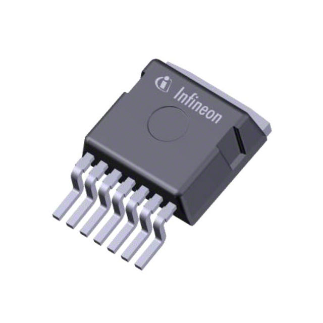
IPBE65R190CFD7AATMA1
Active650 V COOLMOS™ CFD7A AUTOMOTIVE POWER MOSFET D2PAK 7PIN (TO-263 7PIN)
Deep-Dive with AI
Search across all available documentation for this part.

IPBE65R190CFD7AATMA1
Active650 V COOLMOS™ CFD7A AUTOMOTIVE POWER MOSFET D2PAK 7PIN (TO-263 7PIN)
Deep-Dive with AI
Technical Specifications
Parameters and characteristics for this part
| Specification | IPBE65R190CFD7AATMA1 |
|---|---|
| Current - Continuous Drain (Id) @ 25°C | 14 A |
| Drain to Source Voltage (Vdss) | 650 V |
| FET Type | N-Channel |
| Gate Charge (Qg) (Max) @ Vgs | 7 nC |
| Grade | Automotive |
| Input Capacitance (Ciss) (Max) @ Vds | 1291 pF |
| Mounting Type | Surface Mount |
| Operating Temperature [Max] | 150 °C |
| Operating Temperature [Min] | -40 °C |
| Package / Case | D2PAK (7 Leads + Tab), TO-263-8, TO-263CA |
| Power Dissipation (Max) | 77 W |
| Qualification | AEC-Q101 |
| Rds On (Max) @ Id, Vgs | 190 mOhm |
| Supplier Device Package | PG-TO263-7-11 |
| Technology | MOSFET (Metal Oxide) |
| Vgs (Max) | 20 V |
| Vgs(th) (Max) @ Id | 4.5 V |
Pricing
Prices provided here are for design reference only. For realtime values and availability, please visit the distributors directly
Description
General part information
IPBE65 Series
The 190mOhm IPBE65R190CFD7A in D2PAK 7-pin package is part of the automotive-qualified 650V CoolMOS™ SJ powerMOSFET CFD7Aproduct family. As compared to the previous generation, CoolMOS™ CFD7A offers higher reliability and power density while increasing design flexibility. When using Infineon’s 650 VCoolMOS™ CFD7Atechnology in combination with the D2PAK 7-pin package, customers benefit from enhanced efficiency and thermal behavior. The Kelvin-source concept used in the D2PAK 7-pin (driver-source pin) overcomes the limitations caused by the source inductance and improves the switching performance. Resulting advantages at system level, especially at high currents, are the reduction of switching losses and heat. Furthermore, the increased creepage distance of 4.2mm between drain and source/gate facilitates device usage for higher battery voltage classes up to 475V.


