CDCUN1208LPEVM
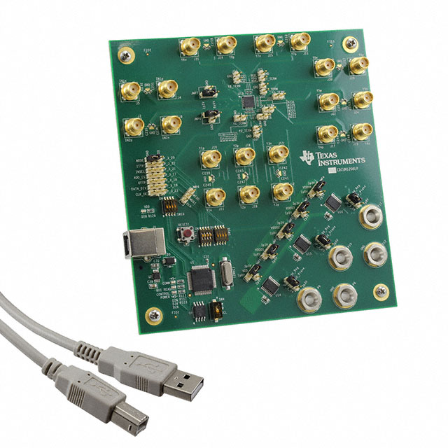
ActiveEVAL MODULE FOR CDCUN1208LP
CDCUN1208LPEVM
ActiveEVAL MODULE FOR CDCUN1208LP
Description
General part information
CDCUN1208 Series
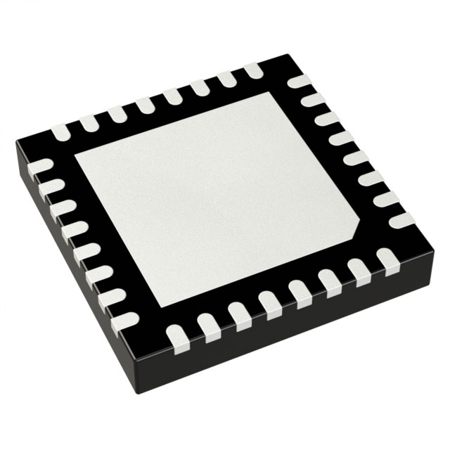
The CDCUN1208LP is a 2:8 fan-out buffer featuring a wide operating supply range, two universal differential/single-ended inputs, and universal outputs (HCSL, LVDS, or LVCMOS) with edge-rate control. The clock buffer supports PCIe Gen1, Gen2 and Gen3. One of the device inputs includes a divider that provides divide values of /1, /2, /4, or /8. The CDCUN1208LP is offered in a 32-pin QFN package, reducing the solution footprint. The device is flexible and easy to use. The state of certain pins determines device configuration at power up. Alternately, the CDCUN1208LP provides a SPI/I2C port with which a host processor controls device settings. The CDCUN1208LP delivers excellent additive jitter performance, and low power consumption. The output section includes four dedicated supply pins enabling the operation of output ports from different power supply domains. This provides the ability to clock devices switching at different LVCMOS levels without the need for external logic level translation circuitry.
The CDCUN1208LP is a 2:8 fan-out buffer featuring a wide operating supply range, two universal differential/single-ended inputs, and universal outputs (HCSL, LVDS, or LVCMOS) with edge-rate control. The clock buffer supports PCIe Gen1, Gen2 and Gen3. One of the device inputs includes a divider that provides divide values of /1, /2, /4, or /8. The CDCUN1208LP is offered in a 32-pin QFN package, reducing the solution footprint. The device is flexible and easy to use. The state of certain pins determines device configuration at power up. Alternately, the CDCUN1208LP provides a SPI/I2C port with which a host processor controls device settings. The CDCUN1208LP delivers excellent additive jitter performance, and low power consumption. The output section includes four dedicated supply pins enabling the operation of output ports from different power supply domains. This provides the ability to clock devices switching at different LVCMOS levels without the need for external logic level translation circuitry.
Technical Specifications
Parameters and characteristics for this part
| Specification | CDCUN1208LPEVM |
|---|---|
| Contents | Board |
| Function | Clock Buffer |
| Primary Attributes | USB Powered or External Supply |
| Secondary Attributes | USB Interfaces, SPI, USB Interface(s) |
| Supplied Contents | Board(s) |
| Type | Timing |
| Utilized IC / Part | CDCUN1208LP |
Pricing
Prices provided here are for design reference only. For realtime values and availability, please visit the distributors directly
Sign in to see pricing
Create a free account to access distributor pricing data.
CAD
3D models and CAD resources for this part
Documents
Technical documentation and resources