TPIC2810D
Active8-BIT LED DRIVER WITH I2C INTERFACE
Deep-Dive with AI
Search across all available documentation for this part.
TPIC2810D
Active8-BIT LED DRIVER WITH I2C INTERFACE
Deep-Dive with AI
Technical Specifications
Parameters and characteristics commom to parts in this series
| Specification | TPIC2810D | TPIC2810 Series |
|---|---|---|
| Current - Output / Channel | 100 mA | 100 mA |
| Frequency | 2 MHz | 2 MHz |
| Internal Switch(s) | True | True |
| Mounting Type | Surface Mount | Surface Mount |
| Number of Outputs | 8 | 8 |
| Operating Temperature [Max] | 150 C | 150 C |
| Operating Temperature [Min] | -40 °C | -40 °C |
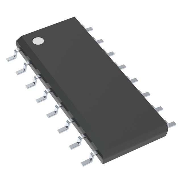
| Package / Case | 16-SOIC | 16-SOIC |
| Package / Case | 3.9 mm Width, 0.154 in | 0.154 - 3.9 mm Width |
| Supplier Device Package | 16-SOIC | 16-SOIC |
| Topology | Shift Register | Shift Register |
| Type | Linear | Linear |
| Voltage - Output | 40 V | 40 V |
| Voltage - Supply (Max) [Max] | 5.5 V | 5.5 V |
| Voltage - Supply (Min) [Min] | 3 V | 3 V |
Pricing
Prices provided here are for design reference only. For realtime values and availability, please visit the distributors directly
TPIC2810 Series
8-bit LED driver with I2C interface
| Part | Number of Outputs | Package / Case | Package / Case | Voltage - Supply (Min) [Min] | Operating Temperature [Max] | Operating Temperature [Min] | Voltage - Supply (Max) [Max] | Mounting Type | Internal Switch(s) | Type | Current - Output / Channel | Supplier Device Package | Voltage - Output | Frequency | Topology |
|---|---|---|---|---|---|---|---|---|---|---|---|---|---|---|---|
Texas Instruments TPIC2810DG4The TPIC2810 device is a monolithic, medium-voltage, low-current, 8-bit shift register design to drive low-side switched resistive loads such as LEDs. The device is not recommended for switching inductive loads.
This device contains an 8-bit, serial-in, parallel-out shift register that feeds an 8-bit D-type storage register. Data transfers through the shift register via an I2C bus interface. Data is transferred into the data shift register only after the group ID and device address have been verified. The subaddress directs the I2C bus interface to read or write data to the device or transfer data to the output. When output enable (G)\ is held high, all drain outputs are off. When G\ is held low, data from the output storage register is transparent to the output buffers. When data in the output buffers is low, the DMOS transistor outputs are off. When data is high, the DMOS transistor outputs have sink-current capability.
The TPIC2810 device has an internal power-up clear to initialize all registers to an off state when power is applied to the device. It also has a thermal sensor to monitor the die temperature and shut the drain outputs off, if an over current condition occurs.
Outputs are low-side, open-drain DMOS transistors with output ratings of 40 V and 100 mA continuous sink-current capability. Each output provides a 210-mA maximum current limit at TC= 25°C. The current limit decreases as the junction temperature increases for additional device protection. The device also provides up to 3000 V of ESD protection on output terminals and 2000 V of ESD protection on input terminals when tested using the human-body model.
The TPIC2810 device is characterized for operation over the operating case temperature range of –40°C to 125°C.
The TPIC2810 device is a monolithic, medium-voltage, low-current, 8-bit shift register design to drive low-side switched resistive loads such as LEDs. The device is not recommended for switching inductive loads.
This device contains an 8-bit, serial-in, parallel-out shift register that feeds an 8-bit D-type storage register. Data transfers through the shift register via an I2C bus interface. Data is transferred into the data shift register only after the group ID and device address have been verified. The subaddress directs the I2C bus interface to read or write data to the device or transfer data to the output. When output enable (G)\ is held high, all drain outputs are off. When G\ is held low, data from the output storage register is transparent to the output buffers. When data in the output buffers is low, the DMOS transistor outputs are off. When data is high, the DMOS transistor outputs have sink-current capability.
The TPIC2810 device has an internal power-up clear to initialize all registers to an off state when power is applied to the device. It also has a thermal sensor to monitor the die temperature and shut the drain outputs off, if an over current condition occurs.
Outputs are low-side, open-drain DMOS transistors with output ratings of 40 V and 100 mA continuous sink-current capability. Each output provides a 210-mA maximum current limit at TC= 25°C. The current limit decreases as the junction temperature increases for additional device protection. The device also provides up to 3000 V of ESD protection on output terminals and 2000 V of ESD protection on input terminals when tested using the human-body model.
The TPIC2810 device is characterized for operation over the operating case temperature range of –40°C to 125°C. | 8 | 16-SOIC | 0.154 in, 3.9 mm Width | 3 V | 150 C | -40 °C | 5.5 V | Surface Mount | Linear | 100 mA | 16-SOIC | 40 V | 2 MHz | Shift Register | |
Texas Instruments TPIC2810DRG4The TPIC2810 device is a monolithic, medium-voltage, low-current, 8-bit shift register design to drive low-side switched resistive loads such as LEDs. The device is not recommended for switching inductive loads.
This device contains an 8-bit, serial-in, parallel-out shift register that feeds an 8-bit D-type storage register. Data transfers through the shift register via an I2C bus interface. Data is transferred into the data shift register only after the group ID and device address have been verified. The subaddress directs the I2C bus interface to read or write data to the device or transfer data to the output. When output enable (G)\ is held high, all drain outputs are off. When G\ is held low, data from the output storage register is transparent to the output buffers. When data in the output buffers is low, the DMOS transistor outputs are off. When data is high, the DMOS transistor outputs have sink-current capability.
The TPIC2810 device has an internal power-up clear to initialize all registers to an off state when power is applied to the device. It also has a thermal sensor to monitor the die temperature and shut the drain outputs off, if an over current condition occurs.
Outputs are low-side, open-drain DMOS transistors with output ratings of 40 V and 100 mA continuous sink-current capability. Each output provides a 210-mA maximum current limit at TC= 25°C. The current limit decreases as the junction temperature increases for additional device protection. The device also provides up to 3000 V of ESD protection on output terminals and 2000 V of ESD protection on input terminals when tested using the human-body model.
The TPIC2810 device is characterized for operation over the operating case temperature range of –40°C to 125°C.
The TPIC2810 device is a monolithic, medium-voltage, low-current, 8-bit shift register design to drive low-side switched resistive loads such as LEDs. The device is not recommended for switching inductive loads.
This device contains an 8-bit, serial-in, parallel-out shift register that feeds an 8-bit D-type storage register. Data transfers through the shift register via an I2C bus interface. Data is transferred into the data shift register only after the group ID and device address have been verified. The subaddress directs the I2C bus interface to read or write data to the device or transfer data to the output. When output enable (G)\ is held high, all drain outputs are off. When G\ is held low, data from the output storage register is transparent to the output buffers. When data in the output buffers is low, the DMOS transistor outputs are off. When data is high, the DMOS transistor outputs have sink-current capability.
The TPIC2810 device has an internal power-up clear to initialize all registers to an off state when power is applied to the device. It also has a thermal sensor to monitor the die temperature and shut the drain outputs off, if an over current condition occurs.
Outputs are low-side, open-drain DMOS transistors with output ratings of 40 V and 100 mA continuous sink-current capability. Each output provides a 210-mA maximum current limit at TC= 25°C. The current limit decreases as the junction temperature increases for additional device protection. The device also provides up to 3000 V of ESD protection on output terminals and 2000 V of ESD protection on input terminals when tested using the human-body model.
The TPIC2810 device is characterized for operation over the operating case temperature range of –40°C to 125°C. | 8 | 16-SOIC | 0.154 in, 3.9 mm Width | 3 V | 150 C | -40 °C | 5.5 V | Surface Mount | Linear | 100 mA | 16-SOIC | 40 V | 2 MHz | Shift Register | |
Texas Instruments TPIC2810DRThe TPIC2810 device is a monolithic, medium-voltage, low-current, 8-bit shift register design to drive low-side switched resistive loads such as LEDs. The device is not recommended for switching inductive loads.
This device contains an 8-bit, serial-in, parallel-out shift register that feeds an 8-bit D-type storage register. Data transfers through the shift register via an I2C bus interface. Data is transferred into the data shift register only after the group ID and device address have been verified. The subaddress directs the I2C bus interface to read or write data to the device or transfer data to the output. When output enable (G)\ is held high, all drain outputs are off. When G\ is held low, data from the output storage register is transparent to the output buffers. When data in the output buffers is low, the DMOS transistor outputs are off. When data is high, the DMOS transistor outputs have sink-current capability.
The TPIC2810 device has an internal power-up clear to initialize all registers to an off state when power is applied to the device. It also has a thermal sensor to monitor the die temperature and shut the drain outputs off, if an over current condition occurs.
Outputs are low-side, open-drain DMOS transistors with output ratings of 40 V and 100 mA continuous sink-current capability. Each output provides a 210-mA maximum current limit at TC= 25°C. The current limit decreases as the junction temperature increases for additional device protection. The device also provides up to 3000 V of ESD protection on output terminals and 2000 V of ESD protection on input terminals when tested using the human-body model.
The TPIC2810 device is characterized for operation over the operating case temperature range of –40°C to 125°C.
The TPIC2810 device is a monolithic, medium-voltage, low-current, 8-bit shift register design to drive low-side switched resistive loads such as LEDs. The device is not recommended for switching inductive loads.
This device contains an 8-bit, serial-in, parallel-out shift register that feeds an 8-bit D-type storage register. Data transfers through the shift register via an I2C bus interface. Data is transferred into the data shift register only after the group ID and device address have been verified. The subaddress directs the I2C bus interface to read or write data to the device or transfer data to the output. When output enable (G)\ is held high, all drain outputs are off. When G\ is held low, data from the output storage register is transparent to the output buffers. When data in the output buffers is low, the DMOS transistor outputs are off. When data is high, the DMOS transistor outputs have sink-current capability.
The TPIC2810 device has an internal power-up clear to initialize all registers to an off state when power is applied to the device. It also has a thermal sensor to monitor the die temperature and shut the drain outputs off, if an over current condition occurs.
Outputs are low-side, open-drain DMOS transistors with output ratings of 40 V and 100 mA continuous sink-current capability. Each output provides a 210-mA maximum current limit at TC= 25°C. The current limit decreases as the junction temperature increases for additional device protection. The device also provides up to 3000 V of ESD protection on output terminals and 2000 V of ESD protection on input terminals when tested using the human-body model.
The TPIC2810 device is characterized for operation over the operating case temperature range of –40°C to 125°C. | 8 | 16-SOIC | 0.154 in, 3.9 mm Width | 3 V | 150 C | -40 °C | 5.5 V | Surface Mount | Linear | 100 mA | 16-SOIC | 40 V | 2 MHz | Shift Register | |
Texas Instruments TPIC2810DThe TPIC2810 device is a monolithic, medium-voltage, low-current, 8-bit shift register design to drive low-side switched resistive loads such as LEDs. The device is not recommended for switching inductive loads.
This device contains an 8-bit, serial-in, parallel-out shift register that feeds an 8-bit D-type storage register. Data transfers through the shift register via an I2C bus interface. Data is transferred into the data shift register only after the group ID and device address have been verified. The subaddress directs the I2C bus interface to read or write data to the device or transfer data to the output. When output enable (G)\ is held high, all drain outputs are off. When G\ is held low, data from the output storage register is transparent to the output buffers. When data in the output buffers is low, the DMOS transistor outputs are off. When data is high, the DMOS transistor outputs have sink-current capability.
The TPIC2810 device has an internal power-up clear to initialize all registers to an off state when power is applied to the device. It also has a thermal sensor to monitor the die temperature and shut the drain outputs off, if an over current condition occurs.
Outputs are low-side, open-drain DMOS transistors with output ratings of 40 V and 100 mA continuous sink-current capability. Each output provides a 210-mA maximum current limit at TC= 25°C. The current limit decreases as the junction temperature increases for additional device protection. The device also provides up to 3000 V of ESD protection on output terminals and 2000 V of ESD protection on input terminals when tested using the human-body model.
The TPIC2810 device is characterized for operation over the operating case temperature range of –40°C to 125°C.
The TPIC2810 device is a monolithic, medium-voltage, low-current, 8-bit shift register design to drive low-side switched resistive loads such as LEDs. The device is not recommended for switching inductive loads.
This device contains an 8-bit, serial-in, parallel-out shift register that feeds an 8-bit D-type storage register. Data transfers through the shift register via an I2C bus interface. Data is transferred into the data shift register only after the group ID and device address have been verified. The subaddress directs the I2C bus interface to read or write data to the device or transfer data to the output. When output enable (G)\ is held high, all drain outputs are off. When G\ is held low, data from the output storage register is transparent to the output buffers. When data in the output buffers is low, the DMOS transistor outputs are off. When data is high, the DMOS transistor outputs have sink-current capability.
The TPIC2810 device has an internal power-up clear to initialize all registers to an off state when power is applied to the device. It also has a thermal sensor to monitor the die temperature and shut the drain outputs off, if an over current condition occurs.
Outputs are low-side, open-drain DMOS transistors with output ratings of 40 V and 100 mA continuous sink-current capability. Each output provides a 210-mA maximum current limit at TC= 25°C. The current limit decreases as the junction temperature increases for additional device protection. The device also provides up to 3000 V of ESD protection on output terminals and 2000 V of ESD protection on input terminals when tested using the human-body model.
The TPIC2810 device is characterized for operation over the operating case temperature range of –40°C to 125°C. | 8 | 16-SOIC | 0.154 in, 3.9 mm Width | 3 V | 150 C | -40 °C | 5.5 V | Surface Mount | Linear | 100 mA | 16-SOIC | 40 V | 2 MHz | Shift Register |
Description
General part information
TPIC2810 Series
The TPIC2810 device is a monolithic, medium-voltage, low-current, 8-bit shift register design to drive low-side switched resistive loads such as LEDs. The device is not recommended for switching inductive loads.
This device contains an 8-bit, serial-in, parallel-out shift register that feeds an 8-bit D-type storage register. Data transfers through the shift register via an I2C bus interface. Data is transferred into the data shift register only after the group ID and device address have been verified. The subaddress directs the I2C bus interface to read or write data to the device or transfer data to the output. When output enable (G)\ is held high, all drain outputs are off. When G\ is held low, data from the output storage register is transparent to the output buffers. When data in the output buffers is low, the DMOS transistor outputs are off. When data is high, the DMOS transistor outputs have sink-current capability.
The TPIC2810 device has an internal power-up clear to initialize all registers to an off state when power is applied to the device. It also has a thermal sensor to monitor the die temperature and shut the drain outputs off, if an over current condition occurs.
Documents
Technical documentation and resources