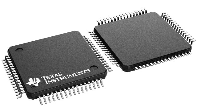
MSC1213Y4PAGT
Active24-BIT, 8-CH DELTA-SIGMA ADC WITH 2X DACS, 8051 MICROCONTROLLER, I<SUP>2</SUP>C AND 16K FLASH MEMORY 64-TQFP -40 TO 125
Deep-Dive with AI
Search across all available documentation for this part.
MSC1213Y4PAGT
Active24-BIT, 8-CH DELTA-SIGMA ADC WITH 2X DACS, 8051 MICROCONTROLLER, I<SUP>2</SUP>C AND 16K FLASH MEMORY 64-TQFP -40 TO 125
Deep-Dive with AI
Technical Specifications
Parameters and characteristics commom to parts in this series
| Specification | MSC1213Y4PAGT | MSC1213 Series |
|---|---|---|
| Data Interface | Parallel, Serial | Parallel, Serial |
| Mounting Type | Surface Mount | Surface Mount |
| Number of Channels | 8 | 8 |
| Operating Temperature [Max] | 125 °C | 125 °C |
| Operating Temperature [Min] | -40 °C | -40 °C |
| Package / Case | 64-TQFP | 64-TQFP |
| Sampling Rate (Per Second) | 1 k | 1 k |
| Supplier Device Package | 64-TQFP (10x10) | 64-TQFP (10x10) |
| Type | ADC and DAC: MCU Based | ADC and DAC: MCU Based |
| Voltage - Supply [Max] | 5.25 V | 5.25 V |
| Voltage - Supply [Min] | 2.7 V | 2.7 V |
| Voltage Supply Source | Analog, Digital | Analog, Digital |
Pricing
Prices provided here are for design reference only. For realtime values and availability, please visit the distributors directly
MSC1213 Series
24-bit, 8-ch delta-sigma ADC with 2x DACs, 8051 microcontroller, I2C and 32k flash memory
| Part | Mounting Type | Package / Case | Number of Channels | Sampling Rate (Per Second) | Supplier Device Package | Voltage Supply Source | Type | Operating Temperature [Max] | Operating Temperature [Min] | Voltage - Supply [Max] | Voltage - Supply [Min] | Data Interface |
|---|---|---|---|---|---|---|---|---|---|---|---|---|
Texas Instruments MSC1213Y2PAGTThe MSC1211/12/13/14 are completely integrated families of mixed-signal devices incorporating a high-resolution delta-sigma () ADC, 16-bit DACs, 8-channel multiplexer, burnout detect current sources, selectable buffered input, offset DAC, Programmable Gain Amplifier (PGA), temperature sensor, voltage reference, 8-bit microcontroller, Flash Program Memory, Flash Data Memory, and Data SRAM.
On-chip peripherals include an additional 32-bit accumulator, an SPI-compatible serial port with FIFO, dual USARTs, multiple digital input/output ports, a watchdog timer, low-voltage detect, on-chip power-on reset, 16-bit PWM, breakpoints, brownout reset, three timer/counters, and a system clock divider. The MSC1211 and MSC1213 also contain a hardware I2C peripheral.
The devices accept low-level differential or single-ended signals directly from a transducer. The ADC provides 24 bits of resolution and 24 bits of no-missing-code performance using a Sinc3filter with a programmable sample rate. The ADC also has a selectable filter that allows for high-resolution, single-cycle conversion.
The microcontroller core is 8051 instruction set compatible. The microcontroller core is an optimized 8051 core that executes up to three times faster than the standard 8051 core, given the same clock source. This design makes it possible to run the devices at a lower external clock frequency and achieve the same performance at lower power than the standard 8051 core.
The MSC1211/12/13/14 allow users to uniquely configure the Flash and SRAM memory maps to meet the needs of their applications. The Flash is programmable down to 2.7V using both serial and parallel programming methods. The Flash endurance is 100k Erase/Write cycles. In addition, 1280 bytes of RAM are incorporated on-chip.
The parts have separate analog and digital supplies, which can be independently powered from 2.7V to +5.25V. At +3V operation, the power dissipation for each part is typically less than 4mW. The MSC1211/12/13/14 are all available in a TQFP-64 package.
The MSC1211/12/13/14 are designed for high-resolution measurement applications in smart transmitters, industrial process control, weigh scales, chromatography, and portable instrumentation.
The MSC1211/12/13/14 are completely integrated families of mixed-signal devices incorporating a high-resolution delta-sigma () ADC, 16-bit DACs, 8-channel multiplexer, burnout detect current sources, selectable buffered input, offset DAC, Programmable Gain Amplifier (PGA), temperature sensor, voltage reference, 8-bit microcontroller, Flash Program Memory, Flash Data Memory, and Data SRAM.
On-chip peripherals include an additional 32-bit accumulator, an SPI-compatible serial port with FIFO, dual USARTs, multiple digital input/output ports, a watchdog timer, low-voltage detect, on-chip power-on reset, 16-bit PWM, breakpoints, brownout reset, three timer/counters, and a system clock divider. The MSC1211 and MSC1213 also contain a hardware I2C peripheral.
The devices accept low-level differential or single-ended signals directly from a transducer. The ADC provides 24 bits of resolution and 24 bits of no-missing-code performance using a Sinc3filter with a programmable sample rate. The ADC also has a selectable filter that allows for high-resolution, single-cycle conversion.
The microcontroller core is 8051 instruction set compatible. The microcontroller core is an optimized 8051 core that executes up to three times faster than the standard 8051 core, given the same clock source. This design makes it possible to run the devices at a lower external clock frequency and achieve the same performance at lower power than the standard 8051 core.
The MSC1211/12/13/14 allow users to uniquely configure the Flash and SRAM memory maps to meet the needs of their applications. The Flash is programmable down to 2.7V using both serial and parallel programming methods. The Flash endurance is 100k Erase/Write cycles. In addition, 1280 bytes of RAM are incorporated on-chip.
The parts have separate analog and digital supplies, which can be independently powered from 2.7V to +5.25V. At +3V operation, the power dissipation for each part is typically less than 4mW. The MSC1211/12/13/14 are all available in a TQFP-64 package.
The MSC1211/12/13/14 are designed for high-resolution measurement applications in smart transmitters, industrial process control, weigh scales, chromatography, and portable instrumentation. | Surface Mount | 64-TQFP | 8 | 1 k | 64-TQFP (10x10) | Analog, Digital | ADC and DAC: MCU Based | 125 °C | -40 °C | 5.25 V | 2.7 V | Parallel, Serial |
Texas Instruments MSC1213Y3PAGTThe MSC1211/12/13/14 are completely integrated families of mixed-signal devices incorporating a high-resolution delta-sigma () ADC, 16-bit DACs, 8-channel multiplexer, burnout detect current sources, selectable buffered input, offset DAC, Programmable Gain Amplifier (PGA), temperature sensor, voltage reference, 8-bit microcontroller, Flash Program Memory, Flash Data Memory, and Data SRAM.
On-chip peripherals include an additional 32-bit accumulator, an SPI-compatible serial port with FIFO, dual USARTs, multiple digital input/output ports, a watchdog timer, low-voltage detect, on-chip power-on reset, 16-bit PWM, breakpoints, brownout reset, three timer/counters, and a system clock divider. The MSC1211 and MSC1213 also contain a hardware I2C peripheral.
The devices accept low-level differential or single-ended signals directly from a transducer. The ADC provides 24 bits of resolution and 24 bits of no-missing-code performance using a Sinc3filter with a programmable sample rate. The ADC also has a selectable filter that allows for high-resolution, single-cycle conversion.
The microcontroller core is 8051 instruction set compatible. The microcontroller core is an optimized 8051 core that executes up to three times faster than the standard 8051 core, given the same clock source. This design makes it possible to run the devices at a lower external clock frequency and achieve the same performance at lower power than the standard 8051 core.
The MSC1211/12/13/14 allow users to uniquely configure the Flash and SRAM memory maps to meet the needs of their applications. The Flash is programmable down to 2.7V using both serial and parallel programming methods. The Flash endurance is 100k Erase/Write cycles. In addition, 1280 bytes of RAM are incorporated on-chip.
The parts have separate analog and digital supplies, which can be independently powered from 2.7V to +5.25V. At +3V operation, the power dissipation for each part is typically less than 4mW. The MSC1211/12/13/14 are all available in a TQFP-64 package.
The MSC1211/12/13/14 are designed for high-resolution measurement applications in smart transmitters, industrial process control, weigh scales, chromatography, and portable instrumentation.
The MSC1211/12/13/14 are completely integrated families of mixed-signal devices incorporating a high-resolution delta-sigma () ADC, 16-bit DACs, 8-channel multiplexer, burnout detect current sources, selectable buffered input, offset DAC, Programmable Gain Amplifier (PGA), temperature sensor, voltage reference, 8-bit microcontroller, Flash Program Memory, Flash Data Memory, and Data SRAM.
On-chip peripherals include an additional 32-bit accumulator, an SPI-compatible serial port with FIFO, dual USARTs, multiple digital input/output ports, a watchdog timer, low-voltage detect, on-chip power-on reset, 16-bit PWM, breakpoints, brownout reset, three timer/counters, and a system clock divider. The MSC1211 and MSC1213 also contain a hardware I2C peripheral.
The devices accept low-level differential or single-ended signals directly from a transducer. The ADC provides 24 bits of resolution and 24 bits of no-missing-code performance using a Sinc3filter with a programmable sample rate. The ADC also has a selectable filter that allows for high-resolution, single-cycle conversion.
The microcontroller core is 8051 instruction set compatible. The microcontroller core is an optimized 8051 core that executes up to three times faster than the standard 8051 core, given the same clock source. This design makes it possible to run the devices at a lower external clock frequency and achieve the same performance at lower power than the standard 8051 core.
The MSC1211/12/13/14 allow users to uniquely configure the Flash and SRAM memory maps to meet the needs of their applications. The Flash is programmable down to 2.7V using both serial and parallel programming methods. The Flash endurance is 100k Erase/Write cycles. In addition, 1280 bytes of RAM are incorporated on-chip.
The parts have separate analog and digital supplies, which can be independently powered from 2.7V to +5.25V. At +3V operation, the power dissipation for each part is typically less than 4mW. The MSC1211/12/13/14 are all available in a TQFP-64 package.
The MSC1211/12/13/14 are designed for high-resolution measurement applications in smart transmitters, industrial process control, weigh scales, chromatography, and portable instrumentation. | Surface Mount | 64-TQFP | 8 | 1 k | 64-TQFP (10x10) | Analog, Digital | ADC and DAC: MCU Based | 125 °C | -40 °C | 5.25 V | 2.7 V | Parallel, Serial |
Surface Mount | 64-TQFP | 8 | 1 k | 64-TQFP (10x10) | Analog, Digital | ADC and DAC: MCU Based | 125 °C | -40 °C | 5.25 V | 2.7 V | Parallel, Serial | |
Texas Instruments MSC1213Y5PAGTThe MSC1211/12/13/14 are completely integrated families of mixed-signal devices incorporating a high-resolution delta-sigma () ADC, 16-bit DACs, 8-channel multiplexer, burnout detect current sources, selectable buffered input, offset DAC, Programmable Gain Amplifier (PGA), temperature sensor, voltage reference, 8-bit microcontroller, Flash Program Memory, Flash Data Memory, and Data SRAM.
On-chip peripherals include an additional 32-bit accumulator, an SPI-compatible serial port with FIFO, dual USARTs, multiple digital input/output ports, a watchdog timer, low-voltage detect, on-chip power-on reset, 16-bit PWM, breakpoints, brownout reset, three timer/counters, and a system clock divider. The MSC1211 and MSC1213 also contain a hardware I2C peripheral.
The devices accept low-level differential or single-ended signals directly from a transducer. The ADC provides 24 bits of resolution and 24 bits of no-missing-code performance using a Sinc3filter with a programmable sample rate. The ADC also has a selectable filter that allows for high-resolution, single-cycle conversion.
The microcontroller core is 8051 instruction set compatible. The microcontroller core is an optimized 8051 core that executes up to three times faster than the standard 8051 core, given the same clock source. This design makes it possible to run the devices at a lower external clock frequency and achieve the same performance at lower power than the standard 8051 core.
The MSC1211/12/13/14 allow users to uniquely configure the Flash and SRAM memory maps to meet the needs of their applications. The Flash is programmable down to 2.7V using both serial and parallel programming methods. The Flash endurance is 100k Erase/Write cycles. In addition, 1280 bytes of RAM are incorporated on-chip.
The parts have separate analog and digital supplies, which can be independently powered from 2.7V to +5.25V. At +3V operation, the power dissipation for each part is typically less than 4mW. The MSC1211/12/13/14 are all available in a TQFP-64 package.
The MSC1211/12/13/14 are designed for high-resolution measurement applications in smart transmitters, industrial process control, weigh scales, chromatography, and portable instrumentation.
The MSC1211/12/13/14 are completely integrated families of mixed-signal devices incorporating a high-resolution delta-sigma () ADC, 16-bit DACs, 8-channel multiplexer, burnout detect current sources, selectable buffered input, offset DAC, Programmable Gain Amplifier (PGA), temperature sensor, voltage reference, 8-bit microcontroller, Flash Program Memory, Flash Data Memory, and Data SRAM.
On-chip peripherals include an additional 32-bit accumulator, an SPI-compatible serial port with FIFO, dual USARTs, multiple digital input/output ports, a watchdog timer, low-voltage detect, on-chip power-on reset, 16-bit PWM, breakpoints, brownout reset, three timer/counters, and a system clock divider. The MSC1211 and MSC1213 also contain a hardware I2C peripheral.
The devices accept low-level differential or single-ended signals directly from a transducer. The ADC provides 24 bits of resolution and 24 bits of no-missing-code performance using a Sinc3filter with a programmable sample rate. The ADC also has a selectable filter that allows for high-resolution, single-cycle conversion.
The microcontroller core is 8051 instruction set compatible. The microcontroller core is an optimized 8051 core that executes up to three times faster than the standard 8051 core, given the same clock source. This design makes it possible to run the devices at a lower external clock frequency and achieve the same performance at lower power than the standard 8051 core.
The MSC1211/12/13/14 allow users to uniquely configure the Flash and SRAM memory maps to meet the needs of their applications. The Flash is programmable down to 2.7V using both serial and parallel programming methods. The Flash endurance is 100k Erase/Write cycles. In addition, 1280 bytes of RAM are incorporated on-chip.
The parts have separate analog and digital supplies, which can be independently powered from 2.7V to +5.25V. At +3V operation, the power dissipation for each part is typically less than 4mW. The MSC1211/12/13/14 are all available in a TQFP-64 package.
The MSC1211/12/13/14 are designed for high-resolution measurement applications in smart transmitters, industrial process control, weigh scales, chromatography, and portable instrumentation. | Surface Mount | 64-TQFP | 8 | 1 k | 64-TQFP (10x10) | Analog, Digital | ADC and DAC: MCU Based | 125 °C | -40 °C | 5.25 V | 2.7 V | Parallel, Serial |
Surface Mount | 64-TQFP | 8 | 1 k | 64-TQFP (10x10) | Analog, Digital | ADC and DAC: MCU Based | 125 °C | -40 °C | 5.25 V | 2.7 V | Parallel, Serial | |
Surface Mount | 64-TQFP | 8 | 1 k | 64-TQFP (10x10) | Analog, Digital | ADC and DAC: MCU Based | 125 °C | -40 °C | 5.25 V | 2.7 V | Parallel, Serial | |
Surface Mount | 64-TQFP | 8 | 1 k | 64-TQFP (10x10) | Analog, Digital | ADC and DAC: MCU Based | 125 °C | -40 °C | 5.25 V | 2.7 V | Parallel, Serial | |
Surface Mount | 64-TQFP | 8 | 1 k | 64-TQFP (10x10) | Analog, Digital | ADC and DAC: MCU Based | 125 °C | -40 °C | 5.25 V | 2.7 V | Parallel, Serial | |
Surface Mount | 64-TQFP | 8 | 1 k | 64-TQFP (10x10) | Analog, Digital | ADC and DAC: MCU Based | 125 °C | -40 °C | 5.25 V | 2.7 V | Parallel, Serial | |
Surface Mount | 64-TQFP | 8 | 1 k | 64-TQFP (10x10) | Analog, Digital | ADC and DAC: MCU Based | 125 °C | -40 °C | 5.25 V | 2.7 V | Parallel, Serial | |
Texas Instruments MSC1213Y4PAGTThe MSC1211/12/13/14 are completely integrated families of mixed-signal devices incorporating a high-resolution delta-sigma () ADC, 16-bit DACs, 8-channel multiplexer, burnout detect current sources, selectable buffered input, offset DAC, Programmable Gain Amplifier (PGA), temperature sensor, voltage reference, 8-bit microcontroller, Flash Program Memory, Flash Data Memory, and Data SRAM.
On-chip peripherals include an additional 32-bit accumulator, an SPI-compatible serial port with FIFO, dual USARTs, multiple digital input/output ports, a watchdog timer, low-voltage detect, on-chip power-on reset, 16-bit PWM, breakpoints, brownout reset, three timer/counters, and a system clock divider. The MSC1211 and MSC1213 also contain a hardware I2C peripheral.
The devices accept low-level differential or single-ended signals directly from a transducer. The ADC provides 24 bits of resolution and 24 bits of no-missing-code performance using a Sinc3filter with a programmable sample rate. The ADC also has a selectable filter that allows for high-resolution, single-cycle conversion.
The microcontroller core is 8051 instruction set compatible. The microcontroller core is an optimized 8051 core that executes up to three times faster than the standard 8051 core, given the same clock source. This design makes it possible to run the devices at a lower external clock frequency and achieve the same performance at lower power than the standard 8051 core.
The MSC1211/12/13/14 allow users to uniquely configure the Flash and SRAM memory maps to meet the needs of their applications. The Flash is programmable down to 2.7V using both serial and parallel programming methods. The Flash endurance is 100k Erase/Write cycles. In addition, 1280 bytes of RAM are incorporated on-chip.
The parts have separate analog and digital supplies, which can be independently powered from 2.7V to +5.25V. At +3V operation, the power dissipation for each part is typically less than 4mW. The MSC1211/12/13/14 are all available in a TQFP-64 package.
The MSC1211/12/13/14 are designed for high-resolution measurement applications in smart transmitters, industrial process control, weigh scales, chromatography, and portable instrumentation.
The MSC1211/12/13/14 are completely integrated families of mixed-signal devices incorporating a high-resolution delta-sigma () ADC, 16-bit DACs, 8-channel multiplexer, burnout detect current sources, selectable buffered input, offset DAC, Programmable Gain Amplifier (PGA), temperature sensor, voltage reference, 8-bit microcontroller, Flash Program Memory, Flash Data Memory, and Data SRAM.
On-chip peripherals include an additional 32-bit accumulator, an SPI-compatible serial port with FIFO, dual USARTs, multiple digital input/output ports, a watchdog timer, low-voltage detect, on-chip power-on reset, 16-bit PWM, breakpoints, brownout reset, three timer/counters, and a system clock divider. The MSC1211 and MSC1213 also contain a hardware I2C peripheral.
The devices accept low-level differential or single-ended signals directly from a transducer. The ADC provides 24 bits of resolution and 24 bits of no-missing-code performance using a Sinc3filter with a programmable sample rate. The ADC also has a selectable filter that allows for high-resolution, single-cycle conversion.
The microcontroller core is 8051 instruction set compatible. The microcontroller core is an optimized 8051 core that executes up to three times faster than the standard 8051 core, given the same clock source. This design makes it possible to run the devices at a lower external clock frequency and achieve the same performance at lower power than the standard 8051 core.
The MSC1211/12/13/14 allow users to uniquely configure the Flash and SRAM memory maps to meet the needs of their applications. The Flash is programmable down to 2.7V using both serial and parallel programming methods. The Flash endurance is 100k Erase/Write cycles. In addition, 1280 bytes of RAM are incorporated on-chip.
The parts have separate analog and digital supplies, which can be independently powered from 2.7V to +5.25V. At +3V operation, the power dissipation for each part is typically less than 4mW. The MSC1211/12/13/14 are all available in a TQFP-64 package.
The MSC1211/12/13/14 are designed for high-resolution measurement applications in smart transmitters, industrial process control, weigh scales, chromatography, and portable instrumentation. | Surface Mount | 64-TQFP | 8 | 1 k | 64-TQFP (10x10) | Analog, Digital | ADC and DAC: MCU Based | 125 °C | -40 °C | 5.25 V | 2.7 V | Parallel, Serial |
Description
General part information
MSC1213 Series
The MSC1211/12/13/14 are completely integrated families of mixed-signal devices incorporating a high-resolution delta-sigma () ADC, 16-bit DACs, 8-channel multiplexer, burnout detect current sources, selectable buffered input, offset DAC, Programmable Gain Amplifier (PGA), temperature sensor, voltage reference, 8-bit microcontroller, Flash Program Memory, Flash Data Memory, and Data SRAM.
On-chip peripherals include an additional 32-bit accumulator, an SPI-compatible serial port with FIFO, dual USARTs, multiple digital input/output ports, a watchdog timer, low-voltage detect, on-chip power-on reset, 16-bit PWM, breakpoints, brownout reset, three timer/counters, and a system clock divider. The MSC1211 and MSC1213 also contain a hardware I2C peripheral.
The devices accept low-level differential or single-ended signals directly from a transducer. The ADC provides 24 bits of resolution and 24 bits of no-missing-code performance using a Sinc3filter with a programmable sample rate. The ADC also has a selectable filter that allows for high-resolution, single-cycle conversion.
Documents
Technical documentation and resources