TPS2819QDBVRQ1
ActiveAUTOMOTIVE 2-A/2-A SINGLE-CHANNEL GATE DRIVER WIH 40-V VDD AND REGULATED OUTPUT 5-SOT-23 -40 TO 125
Deep-Dive with AI
Search across all available documentation for this part.
TPS2819QDBVRQ1
ActiveAUTOMOTIVE 2-A/2-A SINGLE-CHANNEL GATE DRIVER WIH 40-V VDD AND REGULATED OUTPUT 5-SOT-23 -40 TO 125
Deep-Dive with AI
Technical Specifications
Parameters and characteristics for this part
| Specification | TPS2819QDBVRQ1 |
|---|---|
| Channel Type | Single |
| Current - Peak Output (Source, Sink) [custom] | 2 A |
| Current - Peak Output (Source, Sink) [custom] | 2 A |
| Driven Configuration | Low-Side |
| Gate Type | N-Channel MOSFET |
| Grade | Automotive |
| Input Type | Non-Inverting |
| Logic Voltage - VIL, VIH [custom] | 1 V |
| Logic Voltage - VIL, VIH [custom] | 4 V |
| Mounting Type | Surface Mount |
| Number of Drivers | 1 |
| Operating Temperature [Max] | 125 ¯C |
| Operating Temperature [Min] | -40 °C |
| Package / Case | SOT-753, SC-74A |
| Qualification | AEC-Q100 |
| Rise / Fall Time (Typ) [custom] | 14 ns |
| Rise / Fall Time (Typ) [custom] | 14 ns |
| Supplier Device Package | SOT-23-5 |
| Voltage - Supply [Max] | 14 V |
| Voltage - Supply [Min] | 4 V |
Pricing
Prices provided here are for design reference only. For realtime values and availability, please visit the distributors directly
TPS2819-Q1 Series
Automotive 2-A/2-A single-channel gate driver wih 40-V VDD and regulated output
| Part | Gate Type | Mounting Type | Grade | Voltage - Supply [Max] | Voltage - Supply [Min] | Current - Peak Output (Source, Sink) [custom] | Current - Peak Output (Source, Sink) [custom] | Channel Type | Driven Configuration | Supplier Device Package | Package / Case | Number of Drivers | Input Type | Logic Voltage - VIL, VIH [custom] | Logic Voltage - VIL, VIH [custom] | Rise / Fall Time (Typ) [custom] | Rise / Fall Time (Typ) [custom] | Qualification | Operating Temperature [Max] | Operating Temperature [Min] |
|---|---|---|---|---|---|---|---|---|---|---|---|---|---|---|---|---|---|---|---|---|
Texas Instruments TPS2819QDBVRQ1The TPS28xx single-channel high-speed MOSFET drivers are capable of delivering peak currents of up to 2 A into highly capacitive loads. High switching speeds (trand tf= 14 ns typ) are obtained with the use of BiCMOS outputs. Typical threshold switching voltages are two-thirds and one-third of VCC. The design inherently minimizes shoot-through current.
A regulator is provided on TPS2816 through TPS2819 devices to allow operation with supply inputs between 14V and 40V. The regulator output can be used to power other circuits, provided power dissipation does not exceed package limitations. If the regulator is not required, VDD(the regulator input) should be connected to VCC. The TPS2816 and TPS2817 input circuits include an active pullup circuit to eliminate the need for an external resistor when using open-collector PWM controllers. The TPS2818 and TPS2819 are identical to the TPS2816 and TPS2817, except that the active pullup circuit is omitted. The TPS2828 and TPS2829 are identical to the TPS2818 and TPS2819, except that the internal voltage regulator is omitted, allowing quiescent current to drop to less than 15 µA when the inputs are high or low.
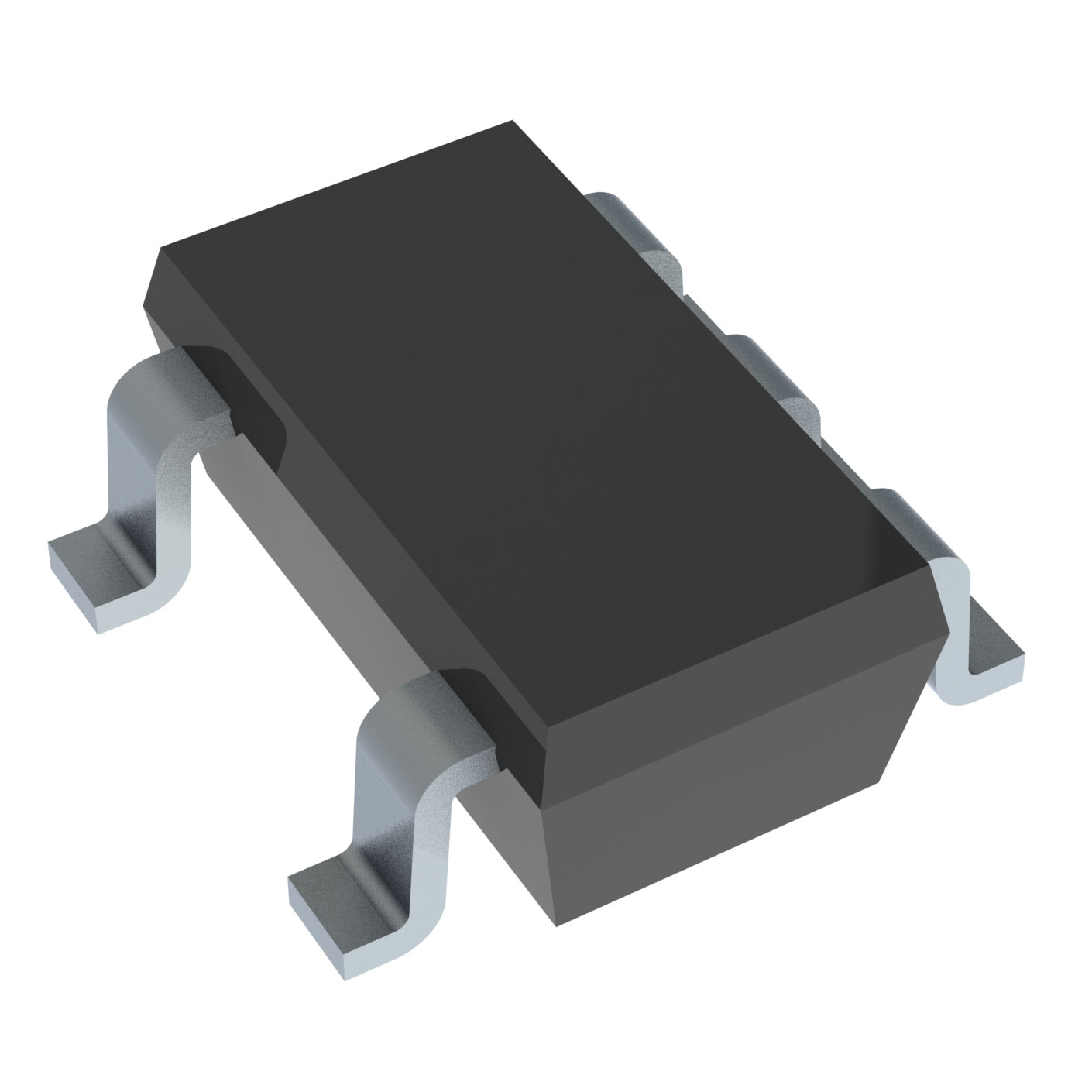
The TPS28xx series devices are available in 5-pin SOT-23 (DBV) packages and operate over an ambient temperature range of –40°C to 125°C.
The TPS28xx single-channel high-speed MOSFET drivers are capable of delivering peak currents of up to 2 A into highly capacitive loads. High switching speeds (trand tf= 14 ns typ) are obtained with the use of BiCMOS outputs. Typical threshold switching voltages are two-thirds and one-third of VCC. The design inherently minimizes shoot-through current.
A regulator is provided on TPS2816 through TPS2819 devices to allow operation with supply inputs between 14V and 40V. The regulator output can be used to power other circuits, provided power dissipation does not exceed package limitations. If the regulator is not required, VDD(the regulator input) should be connected to VCC. The TPS2816 and TPS2817 input circuits include an active pullup circuit to eliminate the need for an external resistor when using open-collector PWM controllers. The TPS2818 and TPS2819 are identical to the TPS2816 and TPS2817, except that the active pullup circuit is omitted. The TPS2828 and TPS2829 are identical to the TPS2818 and TPS2819, except that the internal voltage regulator is omitted, allowing quiescent current to drop to less than 15 µA when the inputs are high or low.
The TPS28xx series devices are available in 5-pin SOT-23 (DBV) packages and operate over an ambient temperature range of –40°C to 125°C. | N-Channel MOSFET | Surface Mount | Automotive | 14 V | 4 V | 2 A | 2 A | Single | Low-Side | SOT-23-5 | SC-74A, SOT-753 | 1 | Non-Inverting | 1 V | 4 V | 14 ns | 14 ns | AEC-Q100 | 125 ¯C | -40 °C |
Description
General part information
TPS2819-Q1 Series
The TPS28xx single-channel high-speed MOSFET drivers are capable of delivering peak currents of up to 2 A into highly capacitive loads. High switching speeds (trand tf= 14 ns typ) are obtained with the use of BiCMOS outputs. Typical threshold switching voltages are two-thirds and one-third of VCC. The design inherently minimizes shoot-through current.
A regulator is provided on TPS2816 through TPS2819 devices to allow operation with supply inputs between 14V and 40V. The regulator output can be used to power other circuits, provided power dissipation does not exceed package limitations. If the regulator is not required, VDD(the regulator input) should be connected to VCC. The TPS2816 and TPS2817 input circuits include an active pullup circuit to eliminate the need for an external resistor when using open-collector PWM controllers. The TPS2818 and TPS2819 are identical to the TPS2816 and TPS2817, except that the active pullup circuit is omitted. The TPS2828 and TPS2829 are identical to the TPS2818 and TPS2819, except that the internal voltage regulator is omitted, allowing quiescent current to drop to less than 15 µA when the inputs are high or low.
The TPS28xx series devices are available in 5-pin SOT-23 (DBV) packages and operate over an ambient temperature range of –40°C to 125°C.
Documents
Technical documentation and resources