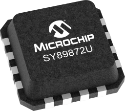
SY89872UMG-TR
Active2.5V LVDS OUTPUT CLOCK DIVIDER/FANOUT
Deep-Dive with AI
Search across all available documentation for this part.

SY89872UMG-TR
Active2.5V LVDS OUTPUT CLOCK DIVIDER/FANOUT
Technical Specifications
Parameters and characteristics commom to parts in this series
| Specification | SY89872UMG-TR | SY89872U Series |
|---|---|---|
| Differential - Input:Output | - | True |
| Differential - Input:Output | - | True |
| Frequency - Max | - | 2 GHz |
| Input | - | LVPECL, HSTL, CML, LVDS |
| Mounting Type | - | Surface Mount |
| null | - | |
| Number of Circuits | - | 1 |
| Operating Temperature | - | 85 °C |
| Operating Temperature | - | -40 °C |
| Output | - | LVDS |
| Package / Case | - | 16-MLF®, 16-VFQFN Exposed Pad |
| Ratio - Input:Output | - | 1:3 |
| Type | - | Divider, Fanout Buffer (Distribution) |
| Voltage - Supply | - | 2.375 V |
| Voltage - Supply | - | 2.625 V |
Pricing
Prices provided here are for design reference only. For realtime values and availability, please visit the distributors directly
| Distributor | Package | Quantity | $ | |
|---|---|---|---|---|
| Microchip Direct | T/R | 1 | $ 13.40 | |
| 25 | $ 11.15 | |||
| 100 | $ 10.15 | |||
| 1000 | $ 8.46 | |||
| 5000 | $ 7.81 | |||
| 10000 | $ 7.26 | |||
SY89872U Series
2.5V LVDS OUTPUT CLOCK DIVIDER/FANOUT
| Part | Number of Circuits | Voltage - Supply [Min] | Voltage - Supply [Max] | Type | Output | Mounting Type | Differential - Input:Output [custom] | Differential - Input:Output [custom] | Frequency - Max [Max] | Ratio - Input:Output [custom] | Package / Case | Input | Operating Temperature [Max] | Operating Temperature [Min] |
|---|---|---|---|---|---|---|---|---|---|---|---|---|---|---|
Microchip Technology SY89872UMG-TR | ||||||||||||||
Microchip Technology SY89872UMG | ||||||||||||||
Microchip Technology SY89872UMG | 1 | 2.375 V | 2.625 V | Divider, Fanout Buffer (Distribution) | LVDS | Surface Mount | 2 GHz | 1:3 | 16-MLF®, 16-VFQFN Exposed Pad | CML, HSTL, LVDS, LVPECL | 85 °C | -40 °C | ||
Microchip Technology SY89872UMG |
Description
General part information
SY89872U Series
This 2.5V low-skew, low-jitter, precision LVDS output clock divider accepts any high-speed differential clock input (AC or DC-coupled) CML, LVPECL, HSTL or LVDS and divides down the frequency using a programmable divider ratio to create a frequency-locked, lower speed version of the input clock. The SY89872U includes two output banks. Bank A is an exact copy of the input clock (pass through) with matched propagation delay to Bank B, the divided output bank.Available divider ratios are 2, 4, 8 and 16. In a typical 622MHz clock system this would provide availability of 311MHz, 155MHz, 77MHz or 38MHz auxiliary clock components.
The differential input buffer has a unique internal termination design that allows access to the termination network through a VT pin. This feature allows the device to easily interface to different logic standards. A VREF- AC reference is included for AC-coupled applications.The SY89872U is part of Micrel's high-speed Precision Edge® timing and distribution family. For 3.3V applications, consider the SY89873L. For applications that require an LVPECL output, consider the SY89872U.The /RESET input asynchronously resets the divider outputs (Bank B). In the pass-through function (Bank A) the /RESET synchronously enables or disables the outputs on the next falling edge of IN (rising edge of /IN). Refer to the "Timing Diagram."
Documents
Technical documentation and resources


