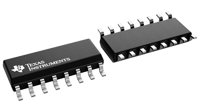
TPL7407LADR
Active30-V, 7-CH NMOS ARRAY LOW-SIDE DRIVER
Deep-Dive with AI
Search across all available documentation for this part.

TPL7407LADR
Active30-V, 7-CH NMOS ARRAY LOW-SIDE DRIVER
Deep-Dive with AI
Technical Specifications
Parameters and characteristics commom to parts in this series
| Specification | TPL7407LADR | TPL7407LA Series |
|---|---|---|
| Current - Output (Max) [Max] | 500 mA | 500 mA |
| Input Type | CMOS | CMOS |
| Interface | Parallel | Parallel |
| Mounting Type | Surface Mount | Surface Mount |
| Number of Outputs | 7 | 7 |
| Operating Temperature [Max] | 125 °C | 125 °C |
| Operating Temperature [Min] | -40 °C | -40 °C |
| Output Configuration | Low Side | Low Side |
| Output Type | N-Channel | N-Channel |
| Package / Case | 16-SOIC | 16-SOIC, 16-TSSOP |
| Package / Case | 3.9 mm Width, 0.154 in | 0.154 - 3.9 mm Width |
| Package / Case | - | 0.173 " |
| Package / Case | - | 4.4 mm |
| Ratio - Input:Output [custom] | 1:1 | 1:1 |
| Supplier Device Package | 16-SOIC | 16-SOIC, 16-TSSOP |
| Switch Type | Solenoid Driver, Relay | Solenoid Driver, Relay |
| Voltage - Load [Max] | 30 V | 30 V |
| Voltage - Supply (Vcc/Vdd) [Max] | 30 V | 30 V |
| Voltage - Supply (Vcc/Vdd) [Min] | 6.5 V | 6.5 V |
Pricing
Prices provided here are for design reference only. For realtime values and availability, please visit the distributors directly
TPL7407LA Series
30-V, 7-ch NMOS array low-side driver
| Part | Input Type | Voltage - Load [Max] | Output Type | Switch Type | Output Configuration | Operating Temperature [Min] | Operating Temperature [Max] | Mounting Type | Number of Outputs | Package / Case | Package / Case | Ratio - Input:Output [custom] | Interface | Supplier Device Package | Voltage - Supply (Vcc/Vdd) [Min] | Voltage - Supply (Vcc/Vdd) [Max] | Current - Output (Max) [Max] | Package / Case [x] | Package / Case [x] |
|---|---|---|---|---|---|---|---|---|---|---|---|---|---|---|---|---|---|---|---|
Texas Instruments TPL7407LADRThe TPL7407LA is a high-voltage, high-current NMOS transistor array. This device consists of seven NMOS transistors that feature high-voltage outputs with common-cathode clamp diodes for switching inductive loads. The maximum drain-current rating of a single NMOS channel is 600 mA. New regulation and drive circuitry added to give maximum drive strength across all GPIO ranges (1.8 V–5 V).The transistors can be paralleled for higher current capability.
The TPL7407LA key benefit is its improved power efficiency and lower leakage than a Bipolar Darlington Implementation. With the lower VOLthe user is dissipating less than half the power than traditional relay drivers with currents less than 250 mA per channel.
The TPL7407LA is a high-voltage, high-current NMOS transistor array. This device consists of seven NMOS transistors that feature high-voltage outputs with common-cathode clamp diodes for switching inductive loads. The maximum drain-current rating of a single NMOS channel is 600 mA. New regulation and drive circuitry added to give maximum drive strength across all GPIO ranges (1.8 V–5 V).The transistors can be paralleled for higher current capability.
The TPL7407LA key benefit is its improved power efficiency and lower leakage than a Bipolar Darlington Implementation. With the lower VOLthe user is dissipating less than half the power than traditional relay drivers with currents less than 250 mA per channel. | CMOS | 30 V | N-Channel | Relay, Solenoid Driver | Low Side | -40 °C | 125 °C | Surface Mount | 7 | 16-SOIC | 0.154 in, 3.9 mm Width | 1:1 | Parallel | 16-SOIC | 6.5 V | 30 V | 500 mA | ||
Texas Instruments TPL7407LAPWRThe TPL7407LA is a high-voltage, high-current NMOS transistor array. This device consists of seven NMOS transistors that feature high-voltage outputs with common-cathode clamp diodes for switching inductive loads. The maximum drain-current rating of a single NMOS channel is 600 mA. New regulation and drive circuitry added to give maximum drive strength across all GPIO ranges (1.8 V–5 V).The transistors can be paralleled for higher current capability.
The TPL7407LA key benefit is its improved power efficiency and lower leakage than a Bipolar Darlington Implementation. With the lower VOLthe user is dissipating less than half the power than traditional relay drivers with currents less than 250 mA per channel.
The TPL7407LA is a high-voltage, high-current NMOS transistor array. This device consists of seven NMOS transistors that feature high-voltage outputs with common-cathode clamp diodes for switching inductive loads. The maximum drain-current rating of a single NMOS channel is 600 mA. New regulation and drive circuitry added to give maximum drive strength across all GPIO ranges (1.8 V–5 V).The transistors can be paralleled for higher current capability.
The TPL7407LA key benefit is its improved power efficiency and lower leakage than a Bipolar Darlington Implementation. With the lower VOLthe user is dissipating less than half the power than traditional relay drivers with currents less than 250 mA per channel. | CMOS | 30 V | N-Channel | Relay, Solenoid Driver | Low Side | -40 °C | 125 °C | Surface Mount | 7 | 16-TSSOP | 1:1 | Parallel | 16-TSSOP | 6.5 V | 30 V | 500 mA | 0.173 " | 4.4 mm |
Description
General part information
TPL7407LA Series
The TPL7407LA is a high-voltage, high-current NMOS transistor array. This device consists of seven NMOS transistors that feature high-voltage outputs with common-cathode clamp diodes for switching inductive loads. The maximum drain-current rating of a single NMOS channel is 600 mA. New regulation and drive circuitry added to give maximum drive strength across all GPIO ranges (1.8 V–5 V).The transistors can be paralleled for higher current capability.
The TPL7407LA key benefit is its improved power efficiency and lower leakage than a Bipolar Darlington Implementation. With the lower VOLthe user is dissipating less than half the power than traditional relay drivers with currents less than 250 mA per channel.
The TPL7407LA is a high-voltage, high-current NMOS transistor array. This device consists of seven NMOS transistors that feature high-voltage outputs with common-cathode clamp diodes for switching inductive loads. The maximum drain-current rating of a single NMOS channel is 600 mA. New regulation and drive circuitry added to give maximum drive strength across all GPIO ranges (1.8 V–5 V).The transistors can be paralleled for higher current capability.
Documents
Technical documentation and resources


