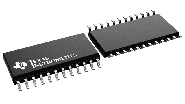
CD74FCT843AM
ActiveBICMOS FCT INTERFACE LOGIC 9-BIT NON-INVERTING TRANSPARENT LATCHES WITH 3-STATE OUTPUTS
Deep-Dive with AI
Search across all available documentation for this part.

CD74FCT843AM
ActiveBICMOS FCT INTERFACE LOGIC 9-BIT NON-INVERTING TRANSPARENT LATCHES WITH 3-STATE OUTPUTS
Deep-Dive with AI
Technical Specifications
Parameters and characteristics commom to parts in this series
| Specification | CD74FCT843AM | 74FCT843 Series |
|---|---|---|
| Circuit [custom] | 9 | 9 |
| Circuit [custom] | 9 | 9 |
| Current - Output High, Low [custom] | 15 mA | 15 mA |
| Current - Output High, Low [custom] | 48 mA | 48 mA |
| Delay Time - Propagation | 9 ns | 9 ns |
| Independent Circuits | 1 | 1 |
| Logic Type | D-Type Transparent Latch | D-Type Transparent Latch |
| Mounting Type | Surface Mount | Surface Mount |
| Operating Temperature [Max] | 70 ░C | 70 ░C |
| Operating Temperature [Min] | 0 °C | 0 °C |
| Output Type | Tri-State | Tri-State |
| Package / Case | 24-SOIC | 24-SOIC |
| Package / Case [x] | 0.295 in | 0.295 in |
| Package / Case [y] | 7.5 mm | 7.5 mm |
| Supplier Device Package | 24-SOIC | 24-SOIC |
| Voltage - Supply [Max] | 5.25 V | 5.25 V |
| Voltage - Supply [Min] | 4.75 V | 4.75 V |
Pricing
Prices provided here are for design reference only. For realtime values and availability, please visit the distributors directly
74FCT843 Series
BiCMOS FCT Interface Logic 9-Bit Non-Inverting Transparent Latches with 3-State Outputs
| Part | Delay Time - Propagation | Voltage - Supply [Min] | Voltage - Supply [Max] | Operating Temperature [Max] | Operating Temperature [Min] | Current - Output High, Low [custom] | Current - Output High, Low [custom] | Output Type | Supplier Device Package | Independent Circuits | Package / Case [y] | Package / Case [x] | Package / Case | Mounting Type | Circuit [custom] | Circuit [custom] | Logic Type |
|---|---|---|---|---|---|---|---|---|---|---|---|---|---|---|---|---|---|
Texas Instruments CD74FCT843AMThe CD74FCT843A is a 9-bit, bus-interface, D-type latch with 3-state outputs, designed specifically for driving highly capacitive or relatively low-impedance loads. It is particularly suitable for implementing buffer registers, I/O ports, bidirectional bus drivers, and working registers.
The device uses a small-geometry BiCMOS technology. The output stage is a combination of bipolar and CMOS transistors that limits the output high level to two diode drops below VCC. This resultant lowering of output swing (0 V to 3.7 V) reduces power-bus ringing [a source of electromagnetic interference (EMI)] and minimizes VCCbounce and ground bounce and their effects during simultaneous output switching. The output configuration also enhances switching speed and is capable of sinking 48 mA.
The CD74FCT843A outputs are transparent to the inputs when the latch-enable (LE) input is high. The latches are transparent D-type latches. When LE goes low, the data is latched. The output-enable (OE\) input controls the 3-state outputs. When OE\ is high, the outputs are in the high-impedance state. The latch operation is independent of the state of the output enable. This device, having preset (PRE\) and clear (CLR\), are ideal for parity-bus interfacing. When PRE\ is low, the outputs are high if OE\ is low. PRE\ overrides CLR\. When CLR\ is low, the outputs are low if OE\ is low. When CLR\ is high, data can be entered into the latch. The device provides noninverted outputs.
OE\ does not affect the internal operations of the latch. Previously stored data can be retained or new data can be entered while the outputs are in the high-impedance state.
The CD74FCT843A is characterized for operation from 0°C to 70°C.
The CD74FCT843A is a 9-bit, bus-interface, D-type latch with 3-state outputs, designed specifically for driving highly capacitive or relatively low-impedance loads. It is particularly suitable for implementing buffer registers, I/O ports, bidirectional bus drivers, and working registers.
The device uses a small-geometry BiCMOS technology. The output stage is a combination of bipolar and CMOS transistors that limits the output high level to two diode drops below VCC. This resultant lowering of output swing (0 V to 3.7 V) reduces power-bus ringing [a source of electromagnetic interference (EMI)] and minimizes VCCbounce and ground bounce and their effects during simultaneous output switching. The output configuration also enhances switching speed and is capable of sinking 48 mA.
The CD74FCT843A outputs are transparent to the inputs when the latch-enable (LE) input is high. The latches are transparent D-type latches. When LE goes low, the data is latched. The output-enable (OE\) input controls the 3-state outputs. When OE\ is high, the outputs are in the high-impedance state. The latch operation is independent of the state of the output enable. This device, having preset (PRE\) and clear (CLR\), are ideal for parity-bus interfacing. When PRE\ is low, the outputs are high if OE\ is low. PRE\ overrides CLR\. When CLR\ is low, the outputs are low if OE\ is low. When CLR\ is high, data can be entered into the latch. The device provides noninverted outputs.
OE\ does not affect the internal operations of the latch. Previously stored data can be retained or new data can be entered while the outputs are in the high-impedance state.
The CD74FCT843A is characterized for operation from 0°C to 70°C. | 9 ns | 4.75 V | 5.25 V | 70 ░C | 0 °C | 15 mA | 48 mA | Tri-State | 24-SOIC | 1 | 7.5 mm | 0.295 in | 24-SOIC | Surface Mount | 9 | 9 | D-Type Transparent Latch |
9 ns | 4.75 V | 5.25 V | 70 ░C | 0 °C | 15 mA | 48 mA | Tri-State | 24-SOIC | 1 | 7.5 mm | 0.295 in | 24-SOIC | Surface Mount | 9 | 9 | D-Type Transparent Latch | |
9 ns | 4.75 V | 5.25 V | 70 ░C | 0 °C | 15 mA | 48 mA | Tri-State | 24-SOIC | 1 | 7.5 mm | 0.295 in | 24-SOIC | Surface Mount | 9 | 9 | D-Type Transparent Latch | |
9 ns | 4.75 V | 5.25 V | 70 ░C | 0 °C | 15 mA | 48 mA | Tri-State | 24-SOIC | 1 | 7.5 mm | 0.295 in | 24-SOIC | Surface Mount | 9 | 9 | D-Type Transparent Latch |
Description
General part information
74FCT843 Series
The CD74FCT843A is a 9-bit, bus-interface, D-type latch with 3-state outputs, designed specifically for driving highly capacitive or relatively low-impedance loads. It is particularly suitable for implementing buffer registers, I/O ports, bidirectional bus drivers, and working registers.
The device uses a small-geometry BiCMOS technology. The output stage is a combination of bipolar and CMOS transistors that limits the output high level to two diode drops below VCC. This resultant lowering of output swing (0 V to 3.7 V) reduces power-bus ringing [a source of electromagnetic interference (EMI)] and minimizes VCCbounce and ground bounce and their effects during simultaneous output switching. The output configuration also enhances switching speed and is capable of sinking 48 mA.
The CD74FCT843A outputs are transparent to the inputs when the latch-enable (LE) input is high. The latches are transparent D-type latches. When LE goes low, the data is latched. The output-enable (OE\) input controls the 3-state outputs. When OE\ is high, the outputs are in the high-impedance state. The latch operation is independent of the state of the output enable. This device, having preset (PRE\) and clear (CLR\), are ideal for parity-bus interfacing. When PRE\ is low, the outputs are high if OE\ is low. PRE\ overrides CLR\. When CLR\ is low, the outputs are low if OE\ is low. When CLR\ is high, data can be entered into the latch. The device provides noninverted outputs.
Documents
Technical documentation and resources


