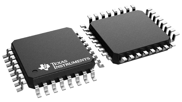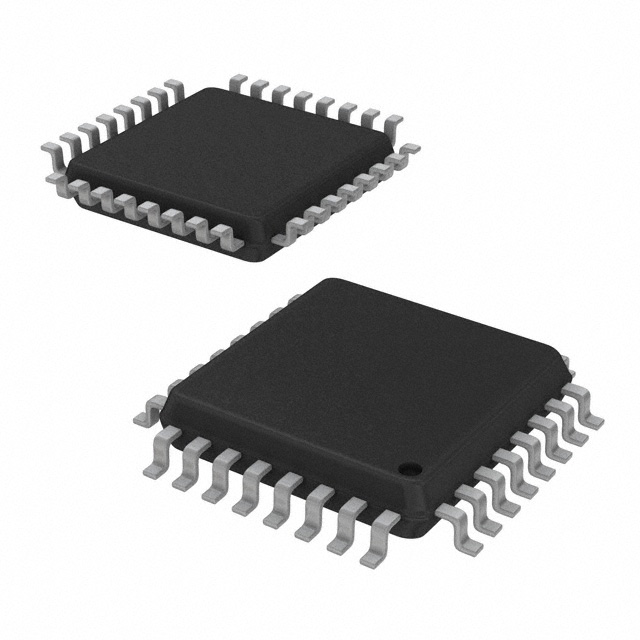
CDCLVP110VFRG4
UnknownCLOCK DRIVER 10-OUT 2-IN 1:10 32-PIN LQFP T/R
CDCLVP110VFRG4
UnknownCLOCK DRIVER 10-OUT 2-IN 1:10 32-PIN LQFP T/R
Description
General part information
CDCLVP110 Series
The CDCLVP110 clock driver distributes one differential clock pair of either LVPECL or HSTL (selectable) input, (CLK0, CLK1) to ten pairs of differential LVPECL clock (Q0, Q9) outputs with minimum skew for clock distribution. The CDCLVP110 can accept two clock sources into an input multiplexer. The CLK0 input accepts either LVECL/LVPECL input signals, while CLK1 accepts an HSTL input signal when operated under LVPECL conditions. The CDCLVP110 is specifically designed for driving 50-Ω transmission lines.
The VBB reference voltage output is used if single-ended input operation is required. In this case the VBB pin should be connected toCLK0and bypassed to GND via a 10-nF capacitor.
However, for high-speed performance up to 3.5 GHz, the differential mode is strongly recommended.
Technical Specifications
Parameters and characteristics for this part
| Specification | CDCLVP110VFRG4 |
|---|---|
| Differential Input | Yes |
| Differential Output | Yes |
| Frequency - Max | 3.5 GHz |
| Input | LVPECL, HSTL |
| Input Ratio | 2 |
| Mounting Type | Surface Mount |
| Number of Circuits | 1 |
| Operating Temperature (Max) | 85 °C |
| Operating Temperature (Min) | -40 °C |
| Output | LVPECL |
| Output Ratio | 10 |
| Package / Case | 32-LQFP |
| Package Length | 7 mm |
| Package Name | 32-LQFP |
| Package Width | 7 mm |
| Type | Multiplexer, Fanout Buffer (Distribution) |
| Voltage - Supply (Maximum) | 3.8 V |
| Voltage - Supply (Minimum) | 2.375 V |
Pricing
Prices provided here are for design reference only. For realtime values and availability, please visit the distributors directly
Sign in to see pricing
Create a free account to access distributor pricing data.
CAD
3D models and CAD resources for this part
Documents
Technical documentation and resources
No documents available