LM5113SDE/NOPB
NRNDDRIVER 5A 2-OUT HIGH SIDE/LOW SIDE HALF BRDG NON-INV 10-PIN WSON EP T/R
LM5113SDE/NOPB
NRNDDRIVER 5A 2-OUT HIGH SIDE/LOW SIDE HALF BRDG NON-INV 10-PIN WSON EP T/R
Description
General part information
LM5113 Series
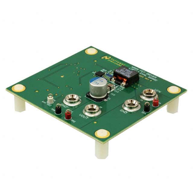
The LM5113 device is designed to drive both the high-side and the low-side enhancement mode Gallium Nitride (GaN) FETs in a synchronous buck or a half bridge configuration. The floating high-side driver is capable of driving a high-side enhancement mode GaN FET operating up to 100 V. The high-side bias voltage is generated using a bootstrap technique and is internally clamped at 5.2 V, which prevents the gate voltage from exceeding the maximum gate-source voltage rating of enhancement mode GaN FETs. The inputs of the LM5113 are TTL logic compatible, and can withstand input voltages up to 14 V regardless of the VDD voltage. The LM5113 has split gate outputs, providing flexibility to adjust the turnon and turnoff strength independently.
The LMG1205 is an enhancement over the LM5113. The LMG1205 takes the design of the LM5113 and includes start-up logic, level shifter, and power-off Vgs clamp enhancements to provide a more robust solution.
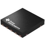
In addition, the strong sink capability of the LM5113 maintains the gate in the low state, preventing unintended turnon during switching. The LM5113 can operate up to several MHz. The LM5113 is available in a standard WSON-10 pin package and a 12-bump DSBGA package. The WSON-10 pin package contains an exposed pad to aid power dissipation. The DSBGA package offers a compact footprint and minimized package inductance.
Technical Specifications
Parameters and characteristics for this part
| Specification | LM5113SDE/NOPB |
|---|---|
| Channel Type | Independent |
| Current - Peak Output (Sink) | 5 A |
| Current - Peak Output (Source) | 1.2 A |
| Driven Configuration | Half-Bridge |
| Fall Time (Typ) | 1.5 ns |
| Gate Channel | N-Channel |
| Gate Type | MOSFET, N-Channel MOSFET |
| High Side Voltage - Max (Bootstrap) | 107 V |
| Input Type | Non-Inverting |
| Logic Voltage - VIH | 1.89 V |
| Logic Voltage - VIL | 1.76 V |
| Mounting Type | Surface Mount |
| Number of Drivers | 2 |
| Operating Temperature (Max) | 125 °C |
| Operating Temperature (Min) | -40 °C |
| Package / Case | 10-WDFN Exposed Pad |
| Package Length | 4 mm |
| Package Name | 10-WSON |
| Package Width | 4 mm |
| Rise Time (Typ) | 7 ns |
| Voltage - Supply (Maximum) | 5.5 V |
| Voltage - Supply (Minimum) | 4.5 V |
Pricing
Prices provided here are for design reference only. For realtime values and availability, please visit the distributors directly
Sign in to see pricing
Create a free account to access distributor pricing data.
CAD
3D models and CAD resources for this part
Documents
Technical documentation and resources