SN75LVDT388ADBT
Active250-MBPS OCTAL LVDS RECEIVER
Deep-Dive with AI
Search across all available documentation for this part.
SN75LVDT388ADBT
Active250-MBPS OCTAL LVDS RECEIVER
Deep-Dive with AI
Technical Specifications
Parameters and characteristics commom to parts in this series
| Specification | SN75LVDT388ADBT | 75LVDT388 Series |
|---|---|---|
| Data Rate | 200 Mbps | 200 Mbps |
| Mounting Type | Surface Mount | Surface Mount |
| Number of Drivers/Receivers [custom] | 8 | 8 |
| Number of Drivers/Receivers [custom] | 0 | 0 |
| Operating Temperature [Max] | 70 ░C | 70 ░C |
| Operating Temperature [Min] | 0 °C | 0 °C |
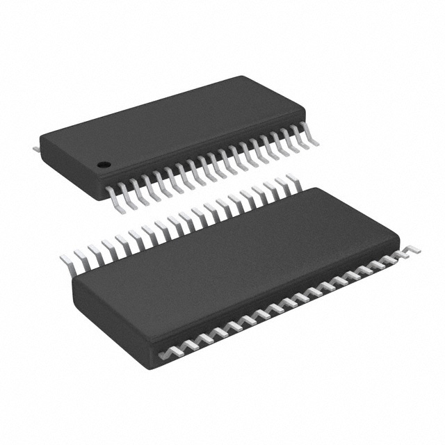
| Package / Case | 4.4 mm | 4.4 mm |
| Package / Case | 38-TFSOP | 38-TFSOP |
| Package / Case | 0.173 in | 0.173 in |
| Protocol | LVDS | LVDS |
| Supplier Device Package | 38-TSSOP | 38-TSSOP |
| Type | Receiver | Receiver |
| Voltage - Supply [Max] | 3.6 V | 3.6 V |
| Voltage - Supply [Min] | 3 V | 3 V |
Pricing
Prices provided here are for design reference only. For realtime values and availability, please visit the distributors directly
75LVDT388 Series
IC RECEIVER 0/8 38TSSOP
| Part | Operating Temperature [Max] | Operating Temperature [Min] | Voltage - Supply [Max] | Voltage - Supply [Min] | Package / Case | Package / Case | Package / Case | Protocol | Number of Drivers/Receivers [custom] | Number of Drivers/Receivers [custom] | Supplier Device Package | Type | Data Rate | Mounting Type |
|---|---|---|---|---|---|---|---|---|---|---|---|---|---|---|
70 ░C | 0 °C | 3.6 V | 3 V | 4.4 mm | 38-TFSOP | 0.173 in | LVDS | 8 | 0 | 38-TSSOP | Receiver | 200 Mbps | Surface Mount | |
Texas Instruments SN75LVDT388ADBTRThis family of 4-, 8-, or 16-differential line receivers (with optional integrated termination) implements the electrical characteristics of low-voltage differential signaling (LVDS). This signaling technique lowers the output voltage levels of 5-V differential standard levels (such as EIA/TIA-422B) to reduce the power, increase the switching speeds, and allow operation with a 3-V supply rail.
Any of the differential receivers provides a valid logical output state with a ±100-mV differential input voltage within the input common-mode voltage range. The input common-mode voltage range allows 1 V of ground potential difference between two LVDS nodes. Additionally, the high-speed switching of LVDS signals almost always requires the use of a line impedance matching resistor at the receiving end of the cable or transmission media. The LVDT products eliminate this external resistor by integrating it with the receiver.
The intended application of this device and signaling technique is for point-to-point baseband data transmission over controlled impedance media of approximately 100 Ω. The transmission media may be printed-circuit board traces, backplanes, or cables. The large number of receivers integrated into the same substrate along with the low pulse skew of balanced signaling, allows extremely precise timing alignment of clock and data for synchronous parallel data transfers. When used with its companion, the 8- or 16-channel driver (the SN65LVDS389 or SN65LVDS387, respectively), over 200 million data transfers per second in single-edge clocked systems are possible with little power.
The ultimate rate and distance of data transfer depends on the attenuation characteristics of the media, the noise coupling to the environment, and other system characteristics.
This family of 4-, 8-, or 16-differential line receivers (with optional integrated termination) implements the electrical characteristics of low-voltage differential signaling (LVDS). This signaling technique lowers the output voltage levels of 5-V differential standard levels (such as EIA/TIA-422B) to reduce the power, increase the switching speeds, and allow operation with a 3-V supply rail.
Any of the differential receivers provides a valid logical output state with a ±100-mV differential input voltage within the input common-mode voltage range. The input common-mode voltage range allows 1 V of ground potential difference between two LVDS nodes. Additionally, the high-speed switching of LVDS signals almost always requires the use of a line impedance matching resistor at the receiving end of the cable or transmission media. The LVDT products eliminate this external resistor by integrating it with the receiver.
The intended application of this device and signaling technique is for point-to-point baseband data transmission over controlled impedance media of approximately 100 Ω. The transmission media may be printed-circuit board traces, backplanes, or cables. The large number of receivers integrated into the same substrate along with the low pulse skew of balanced signaling, allows extremely precise timing alignment of clock and data for synchronous parallel data transfers. When used with its companion, the 8- or 16-channel driver (the SN65LVDS389 or SN65LVDS387, respectively), over 200 million data transfers per second in single-edge clocked systems are possible with little power.
The ultimate rate and distance of data transfer depends on the attenuation characteristics of the media, the noise coupling to the environment, and other system characteristics. | 70 ░C | 0 °C | 3.6 V | 3 V | 4.4 mm | 38-TFSOP | 0.173 in | LVDS | 8 | 0 | 38-TSSOP | Receiver | 200 Mbps | Surface Mount |
Texas Instruments SN75LVDT388ADBTThis family of 4-, 8-, or 16-differential line receivers (with optional integrated termination) implements the electrical characteristics of low-voltage differential signaling (LVDS). This signaling technique lowers the output voltage levels of 5-V differential standard levels (such as EIA/TIA-422B) to reduce the power, increase the switching speeds, and allow operation with a 3-V supply rail.
Any of the differential receivers provides a valid logical output state with a ±100-mV differential input voltage within the input common-mode voltage range. The input common-mode voltage range allows 1 V of ground potential difference between two LVDS nodes. Additionally, the high-speed switching of LVDS signals almost always requires the use of a line impedance matching resistor at the receiving end of the cable or transmission media. The LVDT products eliminate this external resistor by integrating it with the receiver.
The intended application of this device and signaling technique is for point-to-point baseband data transmission over controlled impedance media of approximately 100 Ω. The transmission media may be printed-circuit board traces, backplanes, or cables. The large number of receivers integrated into the same substrate along with the low pulse skew of balanced signaling, allows extremely precise timing alignment of clock and data for synchronous parallel data transfers. When used with its companion, the 8- or 16-channel driver (the SN65LVDS389 or SN65LVDS387, respectively), over 200 million data transfers per second in single-edge clocked systems are possible with little power.
The ultimate rate and distance of data transfer depends on the attenuation characteristics of the media, the noise coupling to the environment, and other system characteristics.
This family of 4-, 8-, or 16-differential line receivers (with optional integrated termination) implements the electrical characteristics of low-voltage differential signaling (LVDS). This signaling technique lowers the output voltage levels of 5-V differential standard levels (such as EIA/TIA-422B) to reduce the power, increase the switching speeds, and allow operation with a 3-V supply rail.
Any of the differential receivers provides a valid logical output state with a ±100-mV differential input voltage within the input common-mode voltage range. The input common-mode voltage range allows 1 V of ground potential difference between two LVDS nodes. Additionally, the high-speed switching of LVDS signals almost always requires the use of a line impedance matching resistor at the receiving end of the cable or transmission media. The LVDT products eliminate this external resistor by integrating it with the receiver.
The intended application of this device and signaling technique is for point-to-point baseband data transmission over controlled impedance media of approximately 100 Ω. The transmission media may be printed-circuit board traces, backplanes, or cables. The large number of receivers integrated into the same substrate along with the low pulse skew of balanced signaling, allows extremely precise timing alignment of clock and data for synchronous parallel data transfers. When used with its companion, the 8- or 16-channel driver (the SN65LVDS389 or SN65LVDS387, respectively), over 200 million data transfers per second in single-edge clocked systems are possible with little power.
The ultimate rate and distance of data transfer depends on the attenuation characteristics of the media, the noise coupling to the environment, and other system characteristics. | 70 ░C | 0 °C | 3.6 V | 3 V | 4.4 mm | 38-TFSOP | 0.173 in | LVDS | 8 | 0 | 38-TSSOP | Receiver | 200 Mbps | Surface Mount |
Description
General part information
75LVDT388 Series
This family of 4-, 8-, or 16-differential line receivers (with optional integrated termination) implements the electrical characteristics of low-voltage differential signaling (LVDS). This signaling technique lowers the output voltage levels of 5-V differential standard levels (such as EIA/TIA-422B) to reduce the power, increase the switching speeds, and allow operation with a 3-V supply rail.
Any of the differential receivers provides a valid logical output state with a ±100-mV differential input voltage within the input common-mode voltage range. The input common-mode voltage range allows 1 V of ground potential difference between two LVDS nodes. Additionally, the high-speed switching of LVDS signals almost always requires the use of a line impedance matching resistor at the receiving end of the cable or transmission media. The LVDT products eliminate this external resistor by integrating it with the receiver.
The intended application of this device and signaling technique is for point-to-point baseband data transmission over controlled impedance media of approximately 100 Ω. The transmission media may be printed-circuit board traces, backplanes, or cables. The large number of receivers integrated into the same substrate along with the low pulse skew of balanced signaling, allows extremely precise timing alignment of clock and data for synchronous parallel data transfers. When used with its companion, the 8- or 16-channel driver (the SN65LVDS389 or SN65LVDS387, respectively), over 200 million data transfers per second in single-edge clocked systems are possible with little power.
Documents
Technical documentation and resources