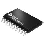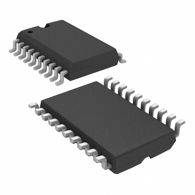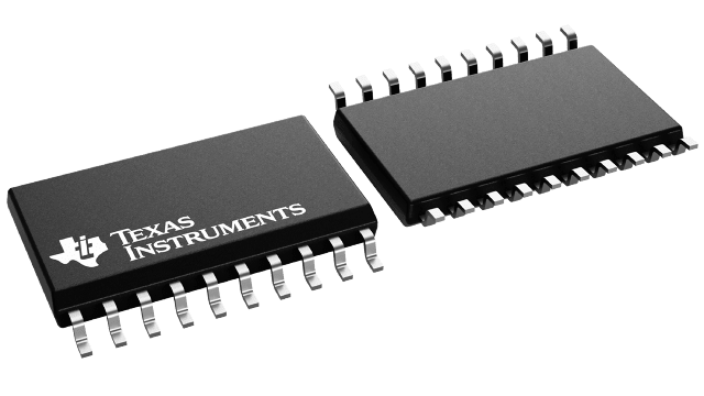
CDC341DWR
Active1-TO-8 TTL CLOCK DRIVER WITH OUTPUT CONTROL PINS FOR LOW STATE
CDC341DWR
Active1-TO-8 TTL CLOCK DRIVER WITH OUTPUT CONTROL PINS FOR LOW STATE
Description
General part information
CDC341 Series
The CDC341 is a high-performance clock-driver circuit that distributes one (A) input signal to eight (Y) outputs with minimum skew for clock distribution. Through the use of the control pins (1G and 2G), the outputs can be placed in a low state regardless of the A input.
The propagation delays are adjusted at the factory using the P0 and P1 pins. These pins are not intended for customer use and should be strapped to GND.
The CDC341 is characterized for operation from 0°C to 70°C.
Technical Specifications
Parameters and characteristics for this part
| Specification | CDC341DWR |
|---|---|
| Differential Input | No |
| Differential Output | No |
| Frequency - Max | 80 MHz |
| Input | TTL |
| Input Ratio | 1 |
| Mounting Type | Surface Mount |
| Number of Circuits | 1 |
| Operating Temperature (Max) | 70 °C |
| Operating Temperature (Min) | 0 °C |
| Output | TTL |
| Output Ratio | 8 |
| Package Length | 0.295 in |
| Package Name | 20-SOIC |
| Package Width | 7.5 mm |
| Type | Fanout Buffer (Distribution) |
| Voltage - Supply (Maximum) | 5.25 V |
| Voltage - Supply (Minimum) | 4.75 V |
Pricing
Prices provided here are for design reference only. For realtime values and availability, please visit the distributors directly
Sign in to see pricing
Create a free account to access distributor pricing data.
CAD
3D models and CAD resources for this part
Documents
Technical documentation and resources