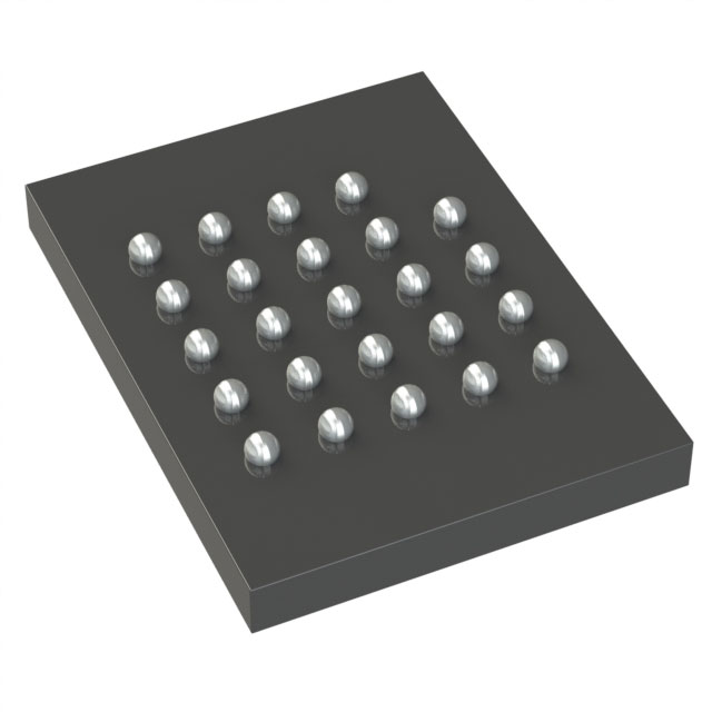
S25FL512SAGBHIA10
ActiveNOR FLASH SERIAL (SPI, DUAL SPI, QUAD SPI) 3V/3.3V 512M-BIT 512M/256M/128M X 1/2-BIT/4-BIT 14.5NS 24-PIN BGA TRAY
Deep-Dive with AI
Search across all available documentation for this part.

S25FL512SAGBHIA10
ActiveNOR FLASH SERIAL (SPI, DUAL SPI, QUAD SPI) 3V/3.3V 512M-BIT 512M/256M/128M X 1/2-BIT/4-BIT 14.5NS 24-PIN BGA TRAY
Deep-Dive with AI
Technical Specifications
Parameters and characteristics for this part
| Specification | S25FL512SAGBHIA10 |
|---|---|
| Clock Frequency | 133 MHz |
| Memory Format | FLASH |
| Memory Interface | SPI - Quad I/O |
| Memory Organization | 64 M |
| Memory Size | 64 MB |
| Memory Type | Non-Volatile |
| Mounting Type | Surface Mount |
| Operating Temperature [Max] | 85 °C |
| Operating Temperature [Min] | -40 °C |
| Package / Case | 24-TBGA |
| Supplier Device Package | 24-BGA |
| Technology | FLASH - NOR |
| Voltage - Supply [Max] | 3.6 V |
| Voltage - Supply [Min] | 2.7 V |
Pricing
Prices provided here are for design reference only. For realtime values and availability, please visit the distributors directly
| Distributor | Package | Quantity | $ | |
|---|---|---|---|---|
| Arrow | N/A | 1 | $ 6.41 | |
| 10 | $ 5.97 | |||
| 25 | $ 5.79 | |||
| 50 | $ 5.59 | |||
| 100 | $ 5.44 | |||
| 250 | $ 5.29 | |||
| 500 | $ 5.08 | |||
| Digikey | Tray | 1 | $ 9.56 | |
| 1 | $ 9.56 | |||
| 10 | $ 8.85 | |||
| 10 | $ 8.85 | |||
| 25 | $ 8.65 | |||
| 25 | $ 8.65 | |||
| 40 | $ 8.60 | |||
| 40 | $ 8.60 | |||
| 80 | $ 7.57 | |||
| 80 | $ 7.57 | |||
| 100 | $ 6.84 | |||
| 100 | $ 6.84 | |||
| 338 | $ 7.20 | |||
| 338 | $ 7.20 | |||
| 676 | $ 7.13 | |||
| 676 | $ 7.13 | |||
| 1014 | $ 6.89 | |||
| 1014 | $ 6.89 | |||
| Newark | Each | 1 | $ 10.24 | |
| 10 | $ 9.28 | |||
| 25 | $ 8.37 | |||
| 50 | $ 8.07 | |||
| 100 | $ 7.77 | |||
| 250 | $ 7.49 | |||
| 500 | $ 7.46 | |||
Description
General part information
S25FL512 Series
S25FL512SAGBHIA10 is a 512Mb serial peripheral interface (SPI) flash memory. This device connects to a host system via an SPI. Traditional SPI single-bit serial input and output (Single I/O or SIO) is supported as well as optional two-bit (Dual I/O or DIO) and four-bit (Quad I/O or QIO) serial commands. This multiple-width interface is called SPI Multi-I/O or MIO. In addition, the FL-S family adds support for double data rate (DDR) read commands for SIO, DIO, and QIO that transfer address and read data on both edges of the clock. The eclipse architecture features a page programming buffer that allows up to 256 words (512 bytes) to be programmed in one operation, resulting in faster effective programming and erase than prior generation SPI programs or erase algorithms. It offers high densities coupled with the flexibility and fast performance required by a variety of embedded applications. It is ideal for code shadowing, XIP, and data storage.
Documents
Technical documentation and resources


