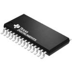
DS90LV110ATMT/NOPB
Active1 TO 10 LVDS DATA/CLOCK DISTRIBUTOR WITH FAILSAFE
DS90LV110ATMT/NOPB
Active1 TO 10 LVDS DATA/CLOCK DISTRIBUTOR WITH FAILSAFE
Description
General part information
DS90LV110 Series
DS90LV110A is a 1 to 10 data/clock distributor utilizing LVDS (Low Voltage Differential Signaling) technology for low power, high speed operation. Data paths are fully differential from input to output for low noise generation and low pulse width distortion. The design allows connection of 1 input to all 10 outputs. LVDS I/O enable high speed data transmission for point-to-point interconnects. This device can be used as a high speed differential 1 to 10 signal distribution / fanout replacing multi-drop bus applications for higher speed links with improved signal quality. It can also be used for clock distribution up to 200MHz.
The DS90LV110A accepts LVDS signal levels, LVPECL levels directly or PECL with attenuation networks.
The LVDS outputs can be put into TRI-STATE by use of the enable pin.
Technical Specifications
Parameters and characteristics for this part
| Specification | DS90LV110ATMT/NOPB |
|---|---|
| Differential Input | Yes |
| Differential Output | Yes |
| Frequency - Max | 200 MHz |
| Input | LVDS, PECL, LVPECL |
| Input Ratio | 1 |
| Mounting Type | Surface Mount |
| Number of Circuits | 1 |
| Operating Temperature (Max) | 85 °C |
| Operating Temperature (Min) | -40 °C |
| Output | LVDS |
| Output Ratio | 10 |
| Package Length | 0.173 in |
| Package Name | 28-TSSOP |
| Package Width | 4.4 mm |
| Type | Fanout Buffer (Distribution) |
| Voltage - Supply (Maximum) | 3.6 V |
| Voltage - Supply (Minimum) | 3 V |
Pricing
Prices provided here are for design reference only. For realtime values and availability, please visit the distributors directly
Sign in to see pricing
Create a free account to access distributor pricing data.
CAD
3D models and CAD resources for this part
Documents
Technical documentation and resources