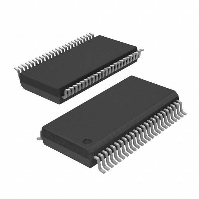
SN74LVCE161284DGGR
Active19-BIT IEEE STD 1284 TRANSLATION TRANSCEIVER WITH ERROR-FREE POWER UP
SN74LVCE161284DGGR
Active19-BIT IEEE STD 1284 TRANSLATION TRANSCEIVER WITH ERROR-FREE POWER UP
Description
General part information
74LVCE161284 Series
The SN74LVCE161284 is designed for 3-V to 3.6-V VCCoperation. This device provides asynchronous two-way communication between data buses. The control-function implementation minimizes external timing requirements.
This device has eight bidirectional bits; data can flow in the A-to-B direction when the direction-control input (DIR) is high and in the B-to-A direction when DIR is low. This device also has five drivers that drive the cable side, and four receivers. The SN74LVCE161284 has one receiver dedicated to the HOST LOGIC line and a driver to drive the PERI LOGIC line.
The output drive mode is determined by the high-drive (HD) control pin. When HD is high, the outputs are in a totem-pole configuration, and in an open-drain configuration when HD is low. This meets the drive requirements as specified in the IEEE Std 1284-I (level-1 type) and IEEE Std 1284-II (level-2 type) parallel peripheral-interface specifications. Except for HOST LOGIC IN and peripheral logic out (PERI LOGIC OUT), all cable-side pins have a 1.4-kintegrated pullup resistor. The pullup resistor is switched off if the associated output driver is in the low state or if the output voltage is above VCCCABLE. If VCCCABLE is off, PERI LOGIC OUT is set to low.
Technical Specifications
Parameters and characteristics for this part
| Specification | SN74LVCE161284DGGR |
|---|---|
| Logic Type | IEEE STD 1284 Translation Transceiver |
| Mounting Type | Surface Mount |
| Number of Bits | 19 bits |
| Operating Temperature (Max) | 70 °C |
| Operating Temperature (Min) | 0 °C |
| Package Length | 0.24 in |
| Package Name | 48-TSSOP, 48-TFSOP |
| Package Width | 6.1 mm |
| Supply Voltage (Max) | 3.6 V |
| Supply Voltage (Min) | 3 V |
Pricing
Prices provided here are for design reference only. For realtime values and availability, please visit the distributors directly
Sign in to see pricing
Create a free account to access distributor pricing data.
CAD
3D models and CAD resources for this part
Documents
Technical documentation and resources