SN74SSTUB32866ZKER
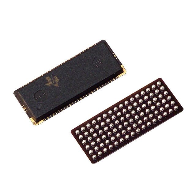
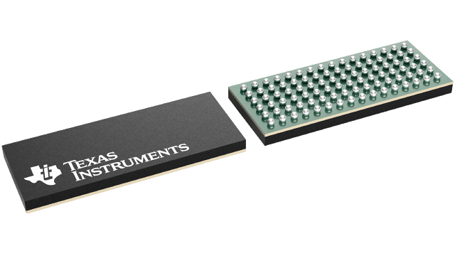
ObsoleteIC CONFIG REG BUFF 25BIT 96-BGA
SN74SSTUB32866ZKER
ObsoleteIC CONFIG REG BUFF 25BIT 96-BGA
Description
General part information
74SSTUB32866 Series
This 25-bit 1:1 or 14-bit 1:2 configurable registered buffer is designed for 1.7-V to 1.9-V VCC operation. In the 1:1 pinout configuration, only one device per DIMM is required to drive nine SDRAM loads. In the 1:2 pinout configuration, two devices per DIMM are required to drive 18 SDRAM loads.
All inputs are SSTL_18, except the reset (RESET) and control (Cn) inputs, which are LVCMOS. All outputs are edge-controlled circuits optimized for unterminated DIMM loads and meet SSTL_18 specifications, except the open-drain error (QERR) output.
The SN74SSTUB32866 operates from a differential clock (CLK andCLK). Data are registered at the crossing of CLK going high and CLK going low.
Technical Specifications
Parameters and characteristics for this part
| Specification | SN74SSTUB32866ZKER |
|---|---|
| Logic Type | 1:2 Configurable Registered Buffer with Parity, Parity, 1:2, Configurable Registered Buffer, 1:1 |
| Mounting Type | Surface Mount |
| Number of Bits | 14, 25 |
| Number of Bits (Max) | 25 bits |
| Number of Bits (Min) | 14 bits |
| Operating Temperature (Max) | 85 °C |
| Operating Temperature (Min) | -40 °C |
| Package / Case | 96-LFBGA |
| Package Length | 13.6 mm |
| Package Name | 96-PBGA MICROSTAR |
| Package Width | 5.6 mm |
| Supply Voltage (Max) | 1.9 V |
| Supply Voltage (Min) | 1.7 V |
Pricing
Prices provided here are for design reference only. For realtime values and availability, please visit the distributors directly
Sign in to see pricing
Create a free account to access distributor pricing data.
CAD
3D models and CAD resources for this part
Documents
Technical documentation and resources
No documents available