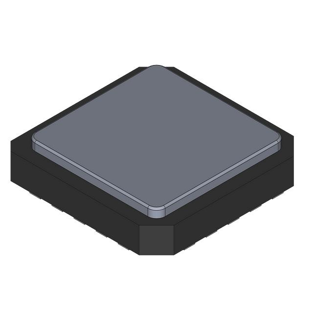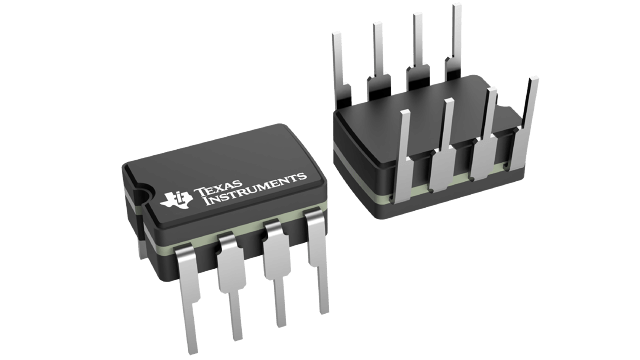
5962-9955702QPA
Active12-BIT, 2.5 US DUAL DAC, SERIAL INPUT, PGRMABLE SETTLING TIME, SIMULTANEOUS UPDATE, LOW POWER
5962-9955702QPA
Active12-BIT, 2.5 US DUAL DAC, SERIAL INPUT, PGRMABLE SETTLING TIME, SIMULTANEOUS UPDATE, LOW POWER
Description
General part information
TLC5618AM Series
The TLC5618 is a dual 12-bit voltage output digital-to-analog converter (DAC) with buffered reference inputs (high impedance). The DACs have an output voltage range that is two times the reference voltage, and the DACs are monotonic. The device is simple to use, running from a single supply of 5 V. A power-on reset function is incorporated in the device to ensure repeatable start-up conditions.
Digital control of the TLC5618 is over a 3-wire CMOS-compatible serial bus. The device receives a 16-bit word for programming and producing the analog output. The digital inputs feature Schmitt triggers for high noise immunity. Digital communication protocols include the SPI™, QSPI™, and Microwire™ standards.
Two versions of the device are available. The TLC5618 does not have an internal state machine and is dependent on all external timing signals. The TLC5618A has an internal state machine that counts the number of clocks from the falling edge of CS\ and then updates and disables the device from accepting further data inputs. The TLC5618A is recommended for TMS320 and SPI processors, and the TLC5618 is recommended only for SPI or 3-wire serial port processors. The TLC5618A is backward-compatible and designed to work in TLC5618 designed systems.
Technical Specifications
Parameters and characteristics for this part
| Specification | 5962-9955702QPA |
|---|---|
| Architecture | String DAC |
| Data Interface | SPI, DSP, Microwire, 3-Wire Serial, QSPI |
| Differential Output | No |
| DNL (LSB) Tolerance | 0.5 LSB |
| DNL (Max) (LSB) | 0.5 LSB |
| INL (Max) (LSB) | 4 LSB |
| Mounting Type | Through Hole |
| Number of Bits | 12 bits |
| Number of D/A Converters | 2 count |
| Operating Temperature (Max) | 125 °C |
| Operating Temperature (Min) | -55 °C |
| Output Type | Voltage - Buffered |
| Package Length | 0.3 in |
| Package Name | 8-CDIP |
| Package Width | 7.62 mm |
| Reference Type | External |
| Settling Time | 12.5 µs |
| Voltage - Supply, Analog (Max) | 5.5 V |
| Voltage - Supply, Analog (Min) | 4.5 V |
| Voltage - Supply, Digital (Max) | 5.5 V |
| Voltage - Supply, Digital (Min) | 4.5 V |
Pricing
Prices provided here are for design reference only. For realtime values and availability, please visit the distributors directly
Sign in to see pricing
Create a free account to access distributor pricing data.
CAD
3D models and CAD resources for this part
Documents
Technical documentation and resources