TPS22925EVM
ActiveEVALUATION MODULE
Deep-Dive with AI
Search across all available documentation for this part.
TPS22925EVM
ActiveEVALUATION MODULE
Deep-Dive with AI
Technical Specifications
Parameters and characteristics commom to parts in this series
| Specification | TPS22925EVM | TPS22925 Series |
|---|---|---|
| Current - Output (Max) | - | 3 A |
| Fault Protection | - | Reverse Current |
| Features | - | Slew Rate Controlled, Load Discharge |
| Function | Power Distribution Switch (Load Switch) | Power Distribution Switch (Load Switch) |
| Input Type | - | Non-Inverting |
| Interface | - | On/Off |
| Mounting Type | - | Surface Mount |
| Number of Outputs | - | 1 |
| Operating Temperature | - | 105 °C |
| Operating Temperature | - | -40 °C |
| Output Configuration | - | High Side |
| Output Type | - | N-Channel |
| Package / Case | - | DSBGA, 6-XFBGA |
| Ratio - Input:Output | - | 1:1 |
| Rds On (Typ) | - | 9.2 mOhm |
| Supplied Contents | Board(s) | Board(s) |
| Supplier Device Package | - | 6-DSBGA |
| Switch Type | - | General Purpose |
| Type | Power Management | Power Management |
| Utilized IC / Part | TPS22925 | TPS22925, TPS22925N |
| Voltage - Load | - | 0.65 V |
| Voltage - Load | - | 3.6 V |
| Voltage - Supply (Vcc/Vdd) | - | Not Required |
Pricing
Prices provided here are for design reference only. For realtime values and availability, please visit the distributors directly
TPS22925 Series
3.6-V, 3-A, 9.2-mΩ load switch with output discharge
| Part | Package / Case | Voltage - Supply (Vcc/Vdd) | Voltage - Load [Min] | Voltage - Load [Max] | Features | Output Type | Interface | Mounting Type | Ratio - Input:Output [custom] | Operating Temperature [Max] | Operating Temperature [Min] | Current - Output (Max) [Max] | Number of Outputs | Switch Type | Supplier Device Package | Input Type | Rds On (Typ) | Output Configuration | Fault Protection | Function | Utilized IC / Part | Type | Supplied Contents |
|---|---|---|---|---|---|---|---|---|---|---|---|---|---|---|---|---|---|---|---|---|---|---|---|
Texas Instruments TPS22925CNYPHRThe TPS22925 product family consists of four devices: TPS22925B, TPS22925BN, TPS22925C, and TPS22925CN. Each device is a 9-mΩ, single-channel load switch with a controlled slew rate.
The devices contain an N–channel MOSFET that can operate over an input voltage range of 0.65 V to 3.6 V and can support a maximum continuous current of 3 A. This continuous current enables the devices to be used across multiple designs and end equipments. Each of the TPS22925 devices provides reverse current blocking when disabled allowing for power supply protection and power multiplexing capabilities.
The controlled rise time for the device greatly reduces inrush current caused by large bulk load capacitances, thereby reducing or eliminating power supply droop. When operating with an input voltage of 3.6 V, the TPS22925Bx devices feature a 97 µs rise time and the TPS22925Cx devices feature an 810 µs rise time.
The TPS22925 family of devices can help reduce the total solution size by offering an optional integrated, 150-Ω pull–down resistor for quick output discharge (QOD) when the switch is turned off. Each of the TPS22925 devices is available in a 0.9 mm × 1.4 mm, 0.5-mm pitch, 0.4-mm height 6–pin wafer chip scale package (WCSP) allowing for smaller, more integrated designs. The WCSP and 9 mΩ of on-resistance allow use in space constrained, battery powered applications. The device is characterized for operation over the free–air temperature range of –40°C to +105°C.
The TPS22925 product family consists of four devices: TPS22925B, TPS22925BN, TPS22925C, and TPS22925CN. Each device is a 9-mΩ, single-channel load switch with a controlled slew rate.
The devices contain an N–channel MOSFET that can operate over an input voltage range of 0.65 V to 3.6 V and can support a maximum continuous current of 3 A. This continuous current enables the devices to be used across multiple designs and end equipments. Each of the TPS22925 devices provides reverse current blocking when disabled allowing for power supply protection and power multiplexing capabilities.
The controlled rise time for the device greatly reduces inrush current caused by large bulk load capacitances, thereby reducing or eliminating power supply droop. When operating with an input voltage of 3.6 V, the TPS22925Bx devices feature a 97 µs rise time and the TPS22925Cx devices feature an 810 µs rise time.
The TPS22925 family of devices can help reduce the total solution size by offering an optional integrated, 150-Ω pull–down resistor for quick output discharge (QOD) when the switch is turned off. Each of the TPS22925 devices is available in a 0.9 mm × 1.4 mm, 0.5-mm pitch, 0.4-mm height 6–pin wafer chip scale package (WCSP) allowing for smaller, more integrated designs. The WCSP and 9 mΩ of on-resistance allow use in space constrained, battery powered applications. The device is characterized for operation over the free–air temperature range of –40°C to +105°C. | 6-XFBGA, DSBGA | Not Required | 0.65 V | 3.6 V | Slew Rate Controlled | N-Channel | On/Off | Surface Mount | 1:1 | 105 °C | -40 °C | 3 A | 1 | General Purpose | 6-DSBGA | Non-Inverting | 9.2 mOhm | High Side | Reverse Current | ||||
Texas Instruments TPS22925CYPHRThe TPS22925 product family consists of four devices: TPS22925B, TPS22925BN, TPS22925C, and TPS22925CN. Each device is a 9-mΩ, single-channel load switch with a controlled slew rate.
The devices contain an N–channel MOSFET that can operate over an input voltage range of 0.65 V to 3.6 V and can support a maximum continuous current of 3 A. This continuous current enables the devices to be used across multiple designs and end equipments. Each of the TPS22925 devices provides reverse current blocking when disabled allowing for power supply protection and power multiplexing capabilities.
The controlled rise time for the device greatly reduces inrush current caused by large bulk load capacitances, thereby reducing or eliminating power supply droop. When operating with an input voltage of 3.6 V, the TPS22925Bx devices feature a 97 µs rise time and the TPS22925Cx devices feature an 810 µs rise time.
The TPS22925 family of devices can help reduce the total solution size by offering an optional integrated, 150-Ω pull–down resistor for quick output discharge (QOD) when the switch is turned off. Each of the TPS22925 devices is available in a 0.9 mm × 1.4 mm, 0.5-mm pitch, 0.4-mm height 6–pin wafer chip scale package (WCSP) allowing for smaller, more integrated designs. The WCSP and 9 mΩ of on-resistance allow use in space constrained, battery powered applications. The device is characterized for operation over the free–air temperature range of –40°C to +105°C.
The TPS22925 product family consists of four devices: TPS22925B, TPS22925BN, TPS22925C, and TPS22925CN. Each device is a 9-mΩ, single-channel load switch with a controlled slew rate.
The devices contain an N–channel MOSFET that can operate over an input voltage range of 0.65 V to 3.6 V and can support a maximum continuous current of 3 A. This continuous current enables the devices to be used across multiple designs and end equipments. Each of the TPS22925 devices provides reverse current blocking when disabled allowing for power supply protection and power multiplexing capabilities.
The controlled rise time for the device greatly reduces inrush current caused by large bulk load capacitances, thereby reducing or eliminating power supply droop. When operating with an input voltage of 3.6 V, the TPS22925Bx devices feature a 97 µs rise time and the TPS22925Cx devices feature an 810 µs rise time.
The TPS22925 family of devices can help reduce the total solution size by offering an optional integrated, 150-Ω pull–down resistor for quick output discharge (QOD) when the switch is turned off. Each of the TPS22925 devices is available in a 0.9 mm × 1.4 mm, 0.5-mm pitch, 0.4-mm height 6–pin wafer chip scale package (WCSP) allowing for smaller, more integrated designs. The WCSP and 9 mΩ of on-resistance allow use in space constrained, battery powered applications. The device is characterized for operation over the free–air temperature range of –40°C to +105°C. | 6-XFBGA, DSBGA | Not Required | 0.65 V | 3.6 V | Load Discharge, Slew Rate Controlled | N-Channel | On/Off | Surface Mount | 1:1 | 105 °C | -40 °C | 3 A | 1 | General Purpose | 6-DSBGA | Non-Inverting | 9.2 mOhm | High Side | Reverse Current | ||||
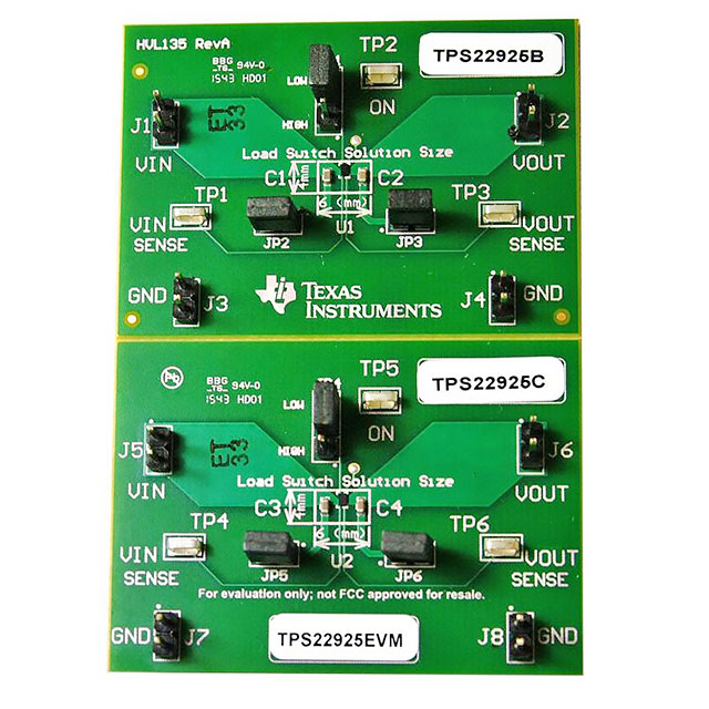
Texas Instruments TPS22925EVMTPS22925 Power Distribution Switch (Load Switch) Power Management Evaluation Board | Power Distribution Switch (Load Switch) | TPS22925 | Power Management | Board(s) | |||||||||||||||||||
Texas Instruments TPS22925BNYPHTThe TPS22925 product family consists of four devices: TPS22925B, TPS22925BN, TPS22925C, and TPS22925CN. Each device is a 9-mΩ, single-channel load switch with a controlled slew rate.
The devices contain an N–channel MOSFET that can operate over an input voltage range of 0.65 V to 3.6 V and can support a maximum continuous current of 3 A. This continuous current enables the devices to be used across multiple designs and end equipments. Each of the TPS22925 devices provides reverse current blocking when disabled allowing for power supply protection and power multiplexing capabilities.
The controlled rise time for the device greatly reduces inrush current caused by large bulk load capacitances, thereby reducing or eliminating power supply droop. When operating with an input voltage of 3.6 V, the TPS22925Bx devices feature a 97 µs rise time and the TPS22925Cx devices feature an 810 µs rise time.
The TPS22925 family of devices can help reduce the total solution size by offering an optional integrated, 150-Ω pull–down resistor for quick output discharge (QOD) when the switch is turned off. Each of the TPS22925 devices is available in a 0.9 mm × 1.4 mm, 0.5-mm pitch, 0.4-mm height 6–pin wafer chip scale package (WCSP) allowing for smaller, more integrated designs. The WCSP and 9 mΩ of on-resistance allow use in space constrained, battery powered applications. The device is characterized for operation over the free–air temperature range of –40°C to +105°C.
The TPS22925 product family consists of four devices: TPS22925B, TPS22925BN, TPS22925C, and TPS22925CN. Each device is a 9-mΩ, single-channel load switch with a controlled slew rate.
The devices contain an N–channel MOSFET that can operate over an input voltage range of 0.65 V to 3.6 V and can support a maximum continuous current of 3 A. This continuous current enables the devices to be used across multiple designs and end equipments. Each of the TPS22925 devices provides reverse current blocking when disabled allowing for power supply protection and power multiplexing capabilities.
The controlled rise time for the device greatly reduces inrush current caused by large bulk load capacitances, thereby reducing or eliminating power supply droop. When operating with an input voltage of 3.6 V, the TPS22925Bx devices feature a 97 µs rise time and the TPS22925Cx devices feature an 810 µs rise time.
The TPS22925 family of devices can help reduce the total solution size by offering an optional integrated, 150-Ω pull–down resistor for quick output discharge (QOD) when the switch is turned off. Each of the TPS22925 devices is available in a 0.9 mm × 1.4 mm, 0.5-mm pitch, 0.4-mm height 6–pin wafer chip scale package (WCSP) allowing for smaller, more integrated designs. The WCSP and 9 mΩ of on-resistance allow use in space constrained, battery powered applications. The device is characterized for operation over the free–air temperature range of –40°C to +105°C. | 6-XFBGA, DSBGA | Not Required | 0.65 V | 3.6 V | Slew Rate Controlled | N-Channel | On/Off | Surface Mount | 1:1 | 105 °C | -40 °C | 3 A | 1 | General Purpose | 6-DSBGA | Non-Inverting | 9.2 mOhm | High Side | Reverse Current | ||||
Texas Instruments TPS22925CNYPHTThe TPS22925 product family consists of four devices: TPS22925B, TPS22925BN, TPS22925C, and TPS22925CN. Each device is a 9-mΩ, single-channel load switch with a controlled slew rate.
The devices contain an N–channel MOSFET that can operate over an input voltage range of 0.65 V to 3.6 V and can support a maximum continuous current of 3 A. This continuous current enables the devices to be used across multiple designs and end equipments. Each of the TPS22925 devices provides reverse current blocking when disabled allowing for power supply protection and power multiplexing capabilities.
The controlled rise time for the device greatly reduces inrush current caused by large bulk load capacitances, thereby reducing or eliminating power supply droop. When operating with an input voltage of 3.6 V, the TPS22925Bx devices feature a 97 µs rise time and the TPS22925Cx devices feature an 810 µs rise time.
The TPS22925 family of devices can help reduce the total solution size by offering an optional integrated, 150-Ω pull–down resistor for quick output discharge (QOD) when the switch is turned off. Each of the TPS22925 devices is available in a 0.9 mm × 1.4 mm, 0.5-mm pitch, 0.4-mm height 6–pin wafer chip scale package (WCSP) allowing for smaller, more integrated designs. The WCSP and 9 mΩ of on-resistance allow use in space constrained, battery powered applications. The device is characterized for operation over the free–air temperature range of –40°C to +105°C.
The TPS22925 product family consists of four devices: TPS22925B, TPS22925BN, TPS22925C, and TPS22925CN. Each device is a 9-mΩ, single-channel load switch with a controlled slew rate.
The devices contain an N–channel MOSFET that can operate over an input voltage range of 0.65 V to 3.6 V and can support a maximum continuous current of 3 A. This continuous current enables the devices to be used across multiple designs and end equipments. Each of the TPS22925 devices provides reverse current blocking when disabled allowing for power supply protection and power multiplexing capabilities.
The controlled rise time for the device greatly reduces inrush current caused by large bulk load capacitances, thereby reducing or eliminating power supply droop. When operating with an input voltage of 3.6 V, the TPS22925Bx devices feature a 97 µs rise time and the TPS22925Cx devices feature an 810 µs rise time.
The TPS22925 family of devices can help reduce the total solution size by offering an optional integrated, 150-Ω pull–down resistor for quick output discharge (QOD) when the switch is turned off. Each of the TPS22925 devices is available in a 0.9 mm × 1.4 mm, 0.5-mm pitch, 0.4-mm height 6–pin wafer chip scale package (WCSP) allowing for smaller, more integrated designs. The WCSP and 9 mΩ of on-resistance allow use in space constrained, battery powered applications. The device is characterized for operation over the free–air temperature range of –40°C to +105°C. | 6-XFBGA, DSBGA | Not Required | 0.65 V | 3.6 V | Slew Rate Controlled | N-Channel | On/Off | Surface Mount | 1:1 | 105 °C | -40 °C | 3 A | 1 | General Purpose | 6-DSBGA | Non-Inverting | 9.2 mOhm | High Side | Reverse Current | ||||
Texas Instruments TPS22925CYPHTThe TPS22925 product family consists of four devices: TPS22925B, TPS22925BN, TPS22925C, and TPS22925CN. Each device is a 9-mΩ, single-channel load switch with a controlled slew rate.
The devices contain an N–channel MOSFET that can operate over an input voltage range of 0.65 V to 3.6 V and can support a maximum continuous current of 3 A. This continuous current enables the devices to be used across multiple designs and end equipments. Each of the TPS22925 devices provides reverse current blocking when disabled allowing for power supply protection and power multiplexing capabilities.
The controlled rise time for the device greatly reduces inrush current caused by large bulk load capacitances, thereby reducing or eliminating power supply droop. When operating with an input voltage of 3.6 V, the TPS22925Bx devices feature a 97 µs rise time and the TPS22925Cx devices feature an 810 µs rise time.
The TPS22925 family of devices can help reduce the total solution size by offering an optional integrated, 150-Ω pull–down resistor for quick output discharge (QOD) when the switch is turned off. Each of the TPS22925 devices is available in a 0.9 mm × 1.4 mm, 0.5-mm pitch, 0.4-mm height 6–pin wafer chip scale package (WCSP) allowing for smaller, more integrated designs. The WCSP and 9 mΩ of on-resistance allow use in space constrained, battery powered applications. The device is characterized for operation over the free–air temperature range of –40°C to +105°C.
The TPS22925 product family consists of four devices: TPS22925B, TPS22925BN, TPS22925C, and TPS22925CN. Each device is a 9-mΩ, single-channel load switch with a controlled slew rate.
The devices contain an N–channel MOSFET that can operate over an input voltage range of 0.65 V to 3.6 V and can support a maximum continuous current of 3 A. This continuous current enables the devices to be used across multiple designs and end equipments. Each of the TPS22925 devices provides reverse current blocking when disabled allowing for power supply protection and power multiplexing capabilities.
The controlled rise time for the device greatly reduces inrush current caused by large bulk load capacitances, thereby reducing or eliminating power supply droop. When operating with an input voltage of 3.6 V, the TPS22925Bx devices feature a 97 µs rise time and the TPS22925Cx devices feature an 810 µs rise time.
The TPS22925 family of devices can help reduce the total solution size by offering an optional integrated, 150-Ω pull–down resistor for quick output discharge (QOD) when the switch is turned off. Each of the TPS22925 devices is available in a 0.9 mm × 1.4 mm, 0.5-mm pitch, 0.4-mm height 6–pin wafer chip scale package (WCSP) allowing for smaller, more integrated designs. The WCSP and 9 mΩ of on-resistance allow use in space constrained, battery powered applications. The device is characterized for operation over the free–air temperature range of –40°C to +105°C. | 6-XFBGA, DSBGA | Not Required | 0.65 V | 3.6 V | Load Discharge, Slew Rate Controlled | N-Channel | On/Off | Surface Mount | 1:1 | 105 °C | -40 °C | 3 A | 1 | General Purpose | 6-DSBGA | Non-Inverting | 9.2 mOhm | High Side | Reverse Current | ||||
Texas Instruments TPS22925BYPHRThe TPS22925 product family consists of four devices: TPS22925B, TPS22925BN, TPS22925C, and TPS22925CN. Each device is a 9-mΩ, single-channel load switch with a controlled slew rate.
The devices contain an N–channel MOSFET that can operate over an input voltage range of 0.65 V to 3.6 V and can support a maximum continuous current of 3 A. This continuous current enables the devices to be used across multiple designs and end equipments. Each of the TPS22925 devices provides reverse current blocking when disabled allowing for power supply protection and power multiplexing capabilities.
The controlled rise time for the device greatly reduces inrush current caused by large bulk load capacitances, thereby reducing or eliminating power supply droop. When operating with an input voltage of 3.6 V, the TPS22925Bx devices feature a 97 µs rise time and the TPS22925Cx devices feature an 810 µs rise time.
The TPS22925 family of devices can help reduce the total solution size by offering an optional integrated, 150-Ω pull–down resistor for quick output discharge (QOD) when the switch is turned off. Each of the TPS22925 devices is available in a 0.9 mm × 1.4 mm, 0.5-mm pitch, 0.4-mm height 6–pin wafer chip scale package (WCSP) allowing for smaller, more integrated designs. The WCSP and 9 mΩ of on-resistance allow use in space constrained, battery powered applications. The device is characterized for operation over the free–air temperature range of –40°C to +105°C.
The TPS22925 product family consists of four devices: TPS22925B, TPS22925BN, TPS22925C, and TPS22925CN. Each device is a 9-mΩ, single-channel load switch with a controlled slew rate.
The devices contain an N–channel MOSFET that can operate over an input voltage range of 0.65 V to 3.6 V and can support a maximum continuous current of 3 A. This continuous current enables the devices to be used across multiple designs and end equipments. Each of the TPS22925 devices provides reverse current blocking when disabled allowing for power supply protection and power multiplexing capabilities.
The controlled rise time for the device greatly reduces inrush current caused by large bulk load capacitances, thereby reducing or eliminating power supply droop. When operating with an input voltage of 3.6 V, the TPS22925Bx devices feature a 97 µs rise time and the TPS22925Cx devices feature an 810 µs rise time.
The TPS22925 family of devices can help reduce the total solution size by offering an optional integrated, 150-Ω pull–down resistor for quick output discharge (QOD) when the switch is turned off. Each of the TPS22925 devices is available in a 0.9 mm × 1.4 mm, 0.5-mm pitch, 0.4-mm height 6–pin wafer chip scale package (WCSP) allowing for smaller, more integrated designs. The WCSP and 9 mΩ of on-resistance allow use in space constrained, battery powered applications. The device is characterized for operation over the free–air temperature range of –40°C to +105°C. | 6-XFBGA, DSBGA | Not Required | 0.65 V | 3.6 V | Load Discharge, Slew Rate Controlled | N-Channel | On/Off | Surface Mount | 1:1 | 105 °C | -40 °C | 3 A | 1 | General Purpose | 6-DSBGA | Non-Inverting | 9.2 mOhm | High Side | Reverse Current | ||||
Texas Instruments TPS22925NEVMTPS22925N Power Distribution Switch (Load Switch) Power Management Evaluation Board | Power Distribution Switch (Load Switch) | TPS22925N | Power Management | Board(s) | |||||||||||||||||||
Texas Instruments TPS22925BYPHTThe TPS22925 product family consists of four devices: TPS22925B, TPS22925BN, TPS22925C, and TPS22925CN. Each device is a 9-mΩ, single-channel load switch with a controlled slew rate.
The devices contain an N–channel MOSFET that can operate over an input voltage range of 0.65 V to 3.6 V and can support a maximum continuous current of 3 A. This continuous current enables the devices to be used across multiple designs and end equipments. Each of the TPS22925 devices provides reverse current blocking when disabled allowing for power supply protection and power multiplexing capabilities.
The controlled rise time for the device greatly reduces inrush current caused by large bulk load capacitances, thereby reducing or eliminating power supply droop. When operating with an input voltage of 3.6 V, the TPS22925Bx devices feature a 97 µs rise time and the TPS22925Cx devices feature an 810 µs rise time.
The TPS22925 family of devices can help reduce the total solution size by offering an optional integrated, 150-Ω pull–down resistor for quick output discharge (QOD) when the switch is turned off. Each of the TPS22925 devices is available in a 0.9 mm × 1.4 mm, 0.5-mm pitch, 0.4-mm height 6–pin wafer chip scale package (WCSP) allowing for smaller, more integrated designs. The WCSP and 9 mΩ of on-resistance allow use in space constrained, battery powered applications. The device is characterized for operation over the free–air temperature range of –40°C to +105°C.
The TPS22925 product family consists of four devices: TPS22925B, TPS22925BN, TPS22925C, and TPS22925CN. Each device is a 9-mΩ, single-channel load switch with a controlled slew rate.
The devices contain an N–channel MOSFET that can operate over an input voltage range of 0.65 V to 3.6 V and can support a maximum continuous current of 3 A. This continuous current enables the devices to be used across multiple designs and end equipments. Each of the TPS22925 devices provides reverse current blocking when disabled allowing for power supply protection and power multiplexing capabilities.
The controlled rise time for the device greatly reduces inrush current caused by large bulk load capacitances, thereby reducing or eliminating power supply droop. When operating with an input voltage of 3.6 V, the TPS22925Bx devices feature a 97 µs rise time and the TPS22925Cx devices feature an 810 µs rise time.
The TPS22925 family of devices can help reduce the total solution size by offering an optional integrated, 150-Ω pull–down resistor for quick output discharge (QOD) when the switch is turned off. Each of the TPS22925 devices is available in a 0.9 mm × 1.4 mm, 0.5-mm pitch, 0.4-mm height 6–pin wafer chip scale package (WCSP) allowing for smaller, more integrated designs. The WCSP and 9 mΩ of on-resistance allow use in space constrained, battery powered applications. The device is characterized for operation over the free–air temperature range of –40°C to +105°C. | 6-XFBGA, DSBGA | Not Required | 0.65 V | 3.6 V | Load Discharge, Slew Rate Controlled | N-Channel | On/Off | Surface Mount | 1:1 | 105 °C | -40 °C | 3 A | 1 | General Purpose | 6-DSBGA | Non-Inverting | 9.2 mOhm | High Side | Reverse Current | ||||
Texas Instruments TPS22925BNYPHRThe TPS22925 product family consists of four devices: TPS22925B, TPS22925BN, TPS22925C, and TPS22925CN. Each device is a 9-mΩ, single-channel load switch with a controlled slew rate.
The devices contain an N–channel MOSFET that can operate over an input voltage range of 0.65 V to 3.6 V and can support a maximum continuous current of 3 A. This continuous current enables the devices to be used across multiple designs and end equipments. Each of the TPS22925 devices provides reverse current blocking when disabled allowing for power supply protection and power multiplexing capabilities.
The controlled rise time for the device greatly reduces inrush current caused by large bulk load capacitances, thereby reducing or eliminating power supply droop. When operating with an input voltage of 3.6 V, the TPS22925Bx devices feature a 97 µs rise time and the TPS22925Cx devices feature an 810 µs rise time.
The TPS22925 family of devices can help reduce the total solution size by offering an optional integrated, 150-Ω pull–down resistor for quick output discharge (QOD) when the switch is turned off. Each of the TPS22925 devices is available in a 0.9 mm × 1.4 mm, 0.5-mm pitch, 0.4-mm height 6–pin wafer chip scale package (WCSP) allowing for smaller, more integrated designs. The WCSP and 9 mΩ of on-resistance allow use in space constrained, battery powered applications. The device is characterized for operation over the free–air temperature range of –40°C to +105°C.
The TPS22925 product family consists of four devices: TPS22925B, TPS22925BN, TPS22925C, and TPS22925CN. Each device is a 9-mΩ, single-channel load switch with a controlled slew rate.
The devices contain an N–channel MOSFET that can operate over an input voltage range of 0.65 V to 3.6 V and can support a maximum continuous current of 3 A. This continuous current enables the devices to be used across multiple designs and end equipments. Each of the TPS22925 devices provides reverse current blocking when disabled allowing for power supply protection and power multiplexing capabilities.
The controlled rise time for the device greatly reduces inrush current caused by large bulk load capacitances, thereby reducing or eliminating power supply droop. When operating with an input voltage of 3.6 V, the TPS22925Bx devices feature a 97 µs rise time and the TPS22925Cx devices feature an 810 µs rise time.
The TPS22925 family of devices can help reduce the total solution size by offering an optional integrated, 150-Ω pull–down resistor for quick output discharge (QOD) when the switch is turned off. Each of the TPS22925 devices is available in a 0.9 mm × 1.4 mm, 0.5-mm pitch, 0.4-mm height 6–pin wafer chip scale package (WCSP) allowing for smaller, more integrated designs. The WCSP and 9 mΩ of on-resistance allow use in space constrained, battery powered applications. The device is characterized for operation over the free–air temperature range of –40°C to +105°C. | 6-XFBGA, DSBGA | Not Required | 0.65 V | 3.6 V | Slew Rate Controlled | N-Channel | On/Off | Surface Mount | 1:1 | 105 °C | -40 °C | 3 A | 1 | General Purpose | 6-DSBGA | Non-Inverting | 9.2 mOhm | High Side | Reverse Current |
Description
General part information
TPS22925 Series
The TPS22925 product family consists of four devices: TPS22925B, TPS22925BN, TPS22925C, and TPS22925CN. Each device is a 9-mΩ, single-channel load switch with a controlled slew rate.
The devices contain an N–channel MOSFET that can operate over an input voltage range of 0.65 V to 3.6 V and can support a maximum continuous current of 3 A. This continuous current enables the devices to be used across multiple designs and end equipments. Each of the TPS22925 devices provides reverse current blocking when disabled allowing for power supply protection and power multiplexing capabilities.
The controlled rise time for the device greatly reduces inrush current caused by large bulk load capacitances, thereby reducing or eliminating power supply droop. When operating with an input voltage of 3.6 V, the TPS22925Bx devices feature a 97 µs rise time and the TPS22925Cx devices feature an 810 µs rise time.
Documents
Technical documentation and resources