DAC8162TDSCR
ActiveDAC8162T DUAL,14-BIT,LOW POWER,VOLTAGE-OUTPUT DACS WITH 2.5-V,4PPM/C, INTERNAL REF, AND 5V TTL I/O
DAC8162TDSCR
ActiveDAC8162T DUAL,14-BIT,LOW POWER,VOLTAGE-OUTPUT DACS WITH 2.5-V,4PPM/C, INTERNAL REF, AND 5V TTL I/O
Description
General part information
DAC8162 Series
The DAC856xT, DAC816xT, and DAC756xT devices are low-power, voltage-output, dual-channel, 16-, 14-, and 12-bit digital-to-analog converters (DACs), respectively. These devices include a 2.5-V, 4-ppm/°C internal reference, giving a full-scale output voltage range of 2.5 V or 5 V. The internal reference has an initial accuracy of ±5 mV and can source or sink up to 20 mA at the VREFIN/VREFOUTpin.
These devices are monotonic, providing excellent linearity and minimizing undesired code-to-code transient voltages (glitch). They use a versatile three-wire serial interface that operates at clock rates up to 50 MHz. The interface is compatible with standard SPI™, QSPI™, Microwire, and digital signal processor (DSP) interfaces. The DACxx62T devices incorporate a power-on-reset circuit that ensures the DAC output powers up and remains at zero scale until a valid code is written to the device, whereas the DACxx63T devices similarly power up at mid-scale. These devices contain a power-down feature that reduces current consumption to typically 550 nA at 5 V. The low power consumption, internal reference, and small footprint make these devices ideal for portable, battery-operated equipment.
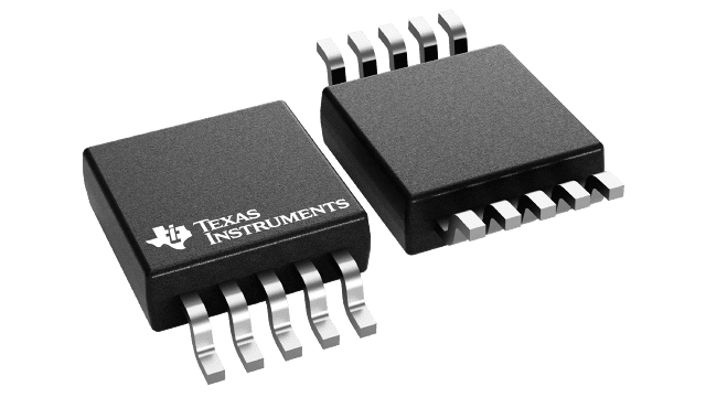
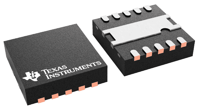
The DACxx62T devices are drop-in and function-compatible with each other, as are the DACxx63T devices. The entire family is available in VSSOP-10 and WSON-10 packages.
Technical Specifications
Parameters and characteristics for this part
| Specification | DAC8162TDSCR |
|---|---|
| Architecture | String DAC |
| Data Interface | DSP, SPI |
| Differential Output | No |
| DNL (LSB) Tolerance | 0.1 LSB |
| INL (LSB) Tolerance | 1 LSB |
| Mounting Type | Surface Mount |
| Number of Bits | 14 bits |
| Number of D/A Converters | 2 count |
| Operating Temperature (Max) | 125 °C |
| Operating Temperature (Min) | -40 °C |
| Output Type | Voltage - Buffered |
| Package / Case | 10-WFDFN Exposed Pad |
| Package Length | 3 mm |
| Package Name | 10-WSON |
| Package Width | 3 mm |
| Reference Type | External, Internal |
| Settling Time (Typical) | 10 µs |
| Voltage - Supply, Analog (Max) | 5.5 V |
| Voltage - Supply, Analog (Min) | 2.7 V |
| Voltage - Supply, Digital (Max) | 5.5 V |
| Voltage - Supply, Digital (Min) | 2.7 V |
Pricing
Prices provided here are for design reference only. For realtime values and availability, please visit the distributors directly
Sign in to see pricing
Create a free account to access distributor pricing data.
CAD
3D models and CAD resources for this part
Documents
Technical documentation and resources