TPS75301QPWPR
Active1.5-A, ULTRA-LOW-DROPOUT VOLTAGE REGULATOR WITH LOW-IQ & RESET WITH DELAY
Deep-Dive with AI
Search across all available documentation for this part.
TPS75301QPWPR
Active1.5-A, ULTRA-LOW-DROPOUT VOLTAGE REGULATOR WITH LOW-IQ & RESET WITH DELAY
Deep-Dive with AI
Technical Specifications
Parameters and characteristics commom to parts in this series
| Specification | TPS75301QPWPR | TPS753 Series |
|---|---|---|
| Control Features | Enable, Power Good, Reset Output | Enable, Power Good, Reset Output |
| Current - Output | 1.5 A | 1.5 A |
| Current - Quiescent (Iq) | 125 µA | 125 µA |
| Mounting Type | Surface Mount | Surface Mount |
| Number of Regulators | 1 | 1 |
| Operating Temperature [Max] | 125 °C | 125 °C |
| Operating Temperature [Min] | -40 °C | -40 °C |
| Output Configuration | Positive | Positive |
| Output Type | Adjustable | Adjustable |
| Output Type | - | 27.03 °C/W |
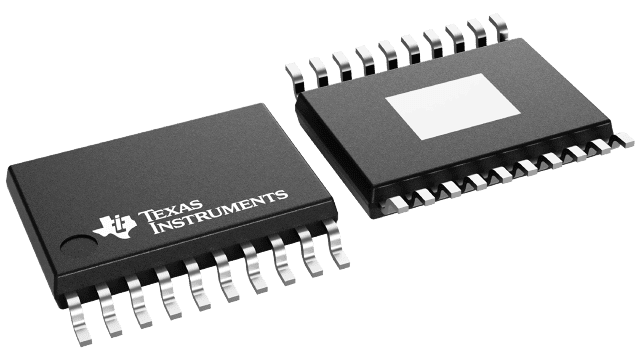
| Package / Case | 20-PowerTSSOP | 20-PowerTSSOP |
| Package / Case [custom] | 0.173 in | 0.173 in |
| Package / Case [custom] | 4.4 mm | 4.4 mm |
| Protection Features | Over Temperature, Reverse Polarity, Over Current | Over Temperature, Reverse Polarity, Over Current |
| PSRR | 63 dB | 60 - 63 dB |
| Supplier Device Package | 20-HTSSOP | 20-HTSSOP |
| Voltage - Input (Max) [Max] | 5.5 V | 5.5 V |
| Voltage - Output (Max) [Max] | 5 V | 5 V |
| Voltage - Output (Min/Fixed) | 1.5 V | 1.5 - 3.3 V |
| Voltage Dropout (Max) | - | 0.3 V |
| Voltage Dropout (Max) [Max] | 0.3 V | 0.3 V |
Pricing
Prices provided here are for design reference only. For realtime values and availability, please visit the distributors directly
TPS753 Series
1.5-A, ultra-low-dropout voltage regulator with low-IQ & RESET with delay
| Part | Number of Regulators | PSRR | Output Type | Current - Quiescent (Iq) | Supplier Device Package | Protection Features | Operating Temperature [Max] | Operating Temperature [Min] | Current - Output | Voltage - Input (Max) [Max] | Mounting Type | Package / Case [custom] | Package / Case | Package / Case [custom] | Control Features | Voltage - Output (Min/Fixed) | Output Configuration | Voltage - Output (Max) [Max] | Output Type | Voltage Dropout (Max) [Max] | Voltage Dropout (Max) |
|---|---|---|---|---|---|---|---|---|---|---|---|---|---|---|---|---|---|---|---|---|---|
Texas Instruments TPS75325QPWPRThe TPS753xxQ and TPS751xxQ devices are low-dropout regulators with integrated power-on reset and power-good (PG) functions respectively. These devices are capable of supplying 1.5 A of output current with a dropout of 160 mV (TPS75133Q, TPS75333Q). Quiescent current is 75 µA at full load and drops down to 1 µA when the device is disabled. These devices are designed to have fast transient response for larger load current changes.
Because the PMOS device behaves as a low-value resistor, the dropout voltage is very low (typically 160 mV at an output current of 1.5 A for the TPS75x33Q) and is directly proportional to the output current. Additionally, because the PMOS pass element is a voltage-driven device, the quiescent current is very low and independent of output loading (typically 75 µA over the full range of output current, 1 mA to 1.5 A). These two key specifications yield a significant improvement in operating life for battery-powered systems.
The device is enabled whenENis connected to a low-level input voltage. This LDO family also features a sleep mode; applying a TTL high signal toEN(enable) shuts down the regulator, reducing the quiescent current to less than 1 µA at TJ= +25°C.
For the TPS751xxQ, the power-good terminal (PG) is an active high, open drain output for use with a power-on reset or a low-battery indicator.
TheRESET(SVS, POR, or power on reset) output of the TPS753xxQ initiates a reset in microcomputer and microprocessor systems in the event of an undervoltage condition. An internal comparator in the TPS753xxQ monitors the output voltage of the regulator to detect an undervoltage condition on the regulated output voltage. When the output reaches 95% of its regulated voltage,RESETgoes to a high-impedance state after a 100-ms delay.RESETgoes to a logic-low state when the regulated output voltage is pulled below 95% (that is, during an overload condition) of its regulated voltage.
The TPS751xxQ and TPS753xxQ are offered in 1.5 V, 1.8 V, 2.5 V and 3.3 V fixed-voltage versions and in an adjustable version (programmable over the range of 1.5 V to 5 V). Output voltage tolerance is specified as a maximum of 2% over line, load, and temperature ranges. The TPS751xxQ and TPS753xxQ families are available in a 20-pin TSSOP (PWP) package.
The TPS753xxQ and TPS751xxQ devices are low-dropout regulators with integrated power-on reset and power-good (PG) functions respectively. These devices are capable of supplying 1.5 A of output current with a dropout of 160 mV (TPS75133Q, TPS75333Q). Quiescent current is 75 µA at full load and drops down to 1 µA when the device is disabled. These devices are designed to have fast transient response for larger load current changes.
Because the PMOS device behaves as a low-value resistor, the dropout voltage is very low (typically 160 mV at an output current of 1.5 A for the TPS75x33Q) and is directly proportional to the output current. Additionally, because the PMOS pass element is a voltage-driven device, the quiescent current is very low and independent of output loading (typically 75 µA over the full range of output current, 1 mA to 1.5 A). These two key specifications yield a significant improvement in operating life for battery-powered systems.
The device is enabled whenENis connected to a low-level input voltage. This LDO family also features a sleep mode; applying a TTL high signal toEN(enable) shuts down the regulator, reducing the quiescent current to less than 1 µA at TJ= +25°C.
For the TPS751xxQ, the power-good terminal (PG) is an active high, open drain output for use with a power-on reset or a low-battery indicator.
TheRESET(SVS, POR, or power on reset) output of the TPS753xxQ initiates a reset in microcomputer and microprocessor systems in the event of an undervoltage condition. An internal comparator in the TPS753xxQ monitors the output voltage of the regulator to detect an undervoltage condition on the regulated output voltage. When the output reaches 95% of its regulated voltage,RESETgoes to a high-impedance state after a 100-ms delay.RESETgoes to a logic-low state when the regulated output voltage is pulled below 95% (that is, during an overload condition) of its regulated voltage.
The TPS751xxQ and TPS753xxQ are offered in 1.5 V, 1.8 V, 2.5 V and 3.3 V fixed-voltage versions and in an adjustable version (programmable over the range of 1.5 V to 5 V). Output voltage tolerance is specified as a maximum of 2% over line, load, and temperature ranges. The TPS751xxQ and TPS753xxQ families are available in a 20-pin TSSOP (PWP) package. | 1 | 60 dB | 27.03 °C/W | 125 µA | 20-HTSSOP | Over Current, Over Temperature, Reverse Polarity | 125 °C | -40 °C | 1.5 A | 5.5 V | Surface Mount | 0.173 in | 20-PowerTSSOP | 4.4 mm | Enable, Power Good, Reset Output | 2.5 V | Positive | ||||
Texas Instruments TPS75301QPWPThe TPS753xxQ and TPS751xxQ devices are low-dropout regulators with integrated power-on reset and power-good (PG) functions respectively. These devices are capable of supplying 1.5 A of output current with a dropout of 160 mV (TPS75133Q, TPS75333Q). Quiescent current is 75 µA at full load and drops down to 1 µA when the device is disabled. These devices are designed to have fast transient response for larger load current changes.
Because the PMOS device behaves as a low-value resistor, the dropout voltage is very low (typically 160 mV at an output current of 1.5 A for the TPS75x33Q) and is directly proportional to the output current. Additionally, because the PMOS pass element is a voltage-driven device, the quiescent current is very low and independent of output loading (typically 75 µA over the full range of output current, 1 mA to 1.5 A). These two key specifications yield a significant improvement in operating life for battery-powered systems.
The device is enabled whenENis connected to a low-level input voltage. This LDO family also features a sleep mode; applying a TTL high signal toEN(enable) shuts down the regulator, reducing the quiescent current to less than 1 µA at TJ= +25°C.
For the TPS751xxQ, the power-good terminal (PG) is an active high, open drain output for use with a power-on reset or a low-battery indicator.
TheRESET(SVS, POR, or power on reset) output of the TPS753xxQ initiates a reset in microcomputer and microprocessor systems in the event of an undervoltage condition. An internal comparator in the TPS753xxQ monitors the output voltage of the regulator to detect an undervoltage condition on the regulated output voltage. When the output reaches 95% of its regulated voltage,RESETgoes to a high-impedance state after a 100-ms delay.RESETgoes to a logic-low state when the regulated output voltage is pulled below 95% (that is, during an overload condition) of its regulated voltage.
The TPS751xxQ and TPS753xxQ are offered in 1.5 V, 1.8 V, 2.5 V and 3.3 V fixed-voltage versions and in an adjustable version (programmable over the range of 1.5 V to 5 V). Output voltage tolerance is specified as a maximum of 2% over line, load, and temperature ranges. The TPS751xxQ and TPS753xxQ families are available in a 20-pin TSSOP (PWP) package.
The TPS753xxQ and TPS751xxQ devices are low-dropout regulators with integrated power-on reset and power-good (PG) functions respectively. These devices are capable of supplying 1.5 A of output current with a dropout of 160 mV (TPS75133Q, TPS75333Q). Quiescent current is 75 µA at full load and drops down to 1 µA when the device is disabled. These devices are designed to have fast transient response for larger load current changes.
Because the PMOS device behaves as a low-value resistor, the dropout voltage is very low (typically 160 mV at an output current of 1.5 A for the TPS75x33Q) and is directly proportional to the output current. Additionally, because the PMOS pass element is a voltage-driven device, the quiescent current is very low and independent of output loading (typically 75 µA over the full range of output current, 1 mA to 1.5 A). These two key specifications yield a significant improvement in operating life for battery-powered systems.
The device is enabled whenENis connected to a low-level input voltage. This LDO family also features a sleep mode; applying a TTL high signal toEN(enable) shuts down the regulator, reducing the quiescent current to less than 1 µA at TJ= +25°C.
For the TPS751xxQ, the power-good terminal (PG) is an active high, open drain output for use with a power-on reset or a low-battery indicator.
TheRESET(SVS, POR, or power on reset) output of the TPS753xxQ initiates a reset in microcomputer and microprocessor systems in the event of an undervoltage condition. An internal comparator in the TPS753xxQ monitors the output voltage of the regulator to detect an undervoltage condition on the regulated output voltage. When the output reaches 95% of its regulated voltage,RESETgoes to a high-impedance state after a 100-ms delay.RESETgoes to a logic-low state when the regulated output voltage is pulled below 95% (that is, during an overload condition) of its regulated voltage.
The TPS751xxQ and TPS753xxQ are offered in 1.5 V, 1.8 V, 2.5 V and 3.3 V fixed-voltage versions and in an adjustable version (programmable over the range of 1.5 V to 5 V). Output voltage tolerance is specified as a maximum of 2% over line, load, and temperature ranges. The TPS751xxQ and TPS753xxQ families are available in a 20-pin TSSOP (PWP) package. | 1 | 63 dB | 125 µA | 20-HTSSOP | Over Current, Over Temperature, Reverse Polarity | 125 °C | -40 °C | 1.5 A | 5.5 V | Surface Mount | 0.173 in | 20-PowerTSSOP | 4.4 mm | Enable, Power Good, Reset Output | 1.5 V | Positive | 5 V | Adjustable | 0.3 V | ||
Texas Instruments TPS75333QPWPThe TPS753xxQ and TPS751xxQ devices are low-dropout regulators with integrated power-on reset and power-good (PG) functions respectively. These devices are capable of supplying 1.5 A of output current with a dropout of 160 mV (TPS75133Q, TPS75333Q). Quiescent current is 75 µA at full load and drops down to 1 µA when the device is disabled. These devices are designed to have fast transient response for larger load current changes.
Because the PMOS device behaves as a low-value resistor, the dropout voltage is very low (typically 160 mV at an output current of 1.5 A for the TPS75x33Q) and is directly proportional to the output current. Additionally, because the PMOS pass element is a voltage-driven device, the quiescent current is very low and independent of output loading (typically 75 µA over the full range of output current, 1 mA to 1.5 A). These two key specifications yield a significant improvement in operating life for battery-powered systems.
The device is enabled whenENis connected to a low-level input voltage. This LDO family also features a sleep mode; applying a TTL high signal toEN(enable) shuts down the regulator, reducing the quiescent current to less than 1 µA at TJ= +25°C.
For the TPS751xxQ, the power-good terminal (PG) is an active high, open drain output for use with a power-on reset or a low-battery indicator.
TheRESET(SVS, POR, or power on reset) output of the TPS753xxQ initiates a reset in microcomputer and microprocessor systems in the event of an undervoltage condition. An internal comparator in the TPS753xxQ monitors the output voltage of the regulator to detect an undervoltage condition on the regulated output voltage. When the output reaches 95% of its regulated voltage,RESETgoes to a high-impedance state after a 100-ms delay.RESETgoes to a logic-low state when the regulated output voltage is pulled below 95% (that is, during an overload condition) of its regulated voltage.
The TPS751xxQ and TPS753xxQ are offered in 1.5 V, 1.8 V, 2.5 V and 3.3 V fixed-voltage versions and in an adjustable version (programmable over the range of 1.5 V to 5 V). Output voltage tolerance is specified as a maximum of 2% over line, load, and temperature ranges. The TPS751xxQ and TPS753xxQ families are available in a 20-pin TSSOP (PWP) package.
The TPS753xxQ and TPS751xxQ devices are low-dropout regulators with integrated power-on reset and power-good (PG) functions respectively. These devices are capable of supplying 1.5 A of output current with a dropout of 160 mV (TPS75133Q, TPS75333Q). Quiescent current is 75 µA at full load and drops down to 1 µA when the device is disabled. These devices are designed to have fast transient response for larger load current changes.
Because the PMOS device behaves as a low-value resistor, the dropout voltage is very low (typically 160 mV at an output current of 1.5 A for the TPS75x33Q) and is directly proportional to the output current. Additionally, because the PMOS pass element is a voltage-driven device, the quiescent current is very low and independent of output loading (typically 75 µA over the full range of output current, 1 mA to 1.5 A). These two key specifications yield a significant improvement in operating life for battery-powered systems.
The device is enabled whenENis connected to a low-level input voltage. This LDO family also features a sleep mode; applying a TTL high signal toEN(enable) shuts down the regulator, reducing the quiescent current to less than 1 µA at TJ= +25°C.
For the TPS751xxQ, the power-good terminal (PG) is an active high, open drain output for use with a power-on reset or a low-battery indicator.
TheRESET(SVS, POR, or power on reset) output of the TPS753xxQ initiates a reset in microcomputer and microprocessor systems in the event of an undervoltage condition. An internal comparator in the TPS753xxQ monitors the output voltage of the regulator to detect an undervoltage condition on the regulated output voltage. When the output reaches 95% of its regulated voltage,RESETgoes to a high-impedance state after a 100-ms delay.RESETgoes to a logic-low state when the regulated output voltage is pulled below 95% (that is, during an overload condition) of its regulated voltage.
The TPS751xxQ and TPS753xxQ are offered in 1.5 V, 1.8 V, 2.5 V and 3.3 V fixed-voltage versions and in an adjustable version (programmable over the range of 1.5 V to 5 V). Output voltage tolerance is specified as a maximum of 2% over line, load, and temperature ranges. The TPS751xxQ and TPS753xxQ families are available in a 20-pin TSSOP (PWP) package. | 1 | 63 dB | 27.03 °C/W | 125 µA | 20-HTSSOP | Over Current, Over Temperature, Reverse Polarity | 125 °C | -40 °C | 1.5 A | 5.5 V | Surface Mount | 0.173 in | 20-PowerTSSOP | 4.4 mm | Enable, Power Good, Reset Output | 3.3 V | Positive | 0.3 V | |||
Texas Instruments TPS75315QPWPThe TPS753xxQ and TPS751xxQ devices are low-dropout regulators with integrated power-on reset and power-good (PG) functions respectively. These devices are capable of supplying 1.5 A of output current with a dropout of 160 mV (TPS75133Q, TPS75333Q). Quiescent current is 75 µA at full load and drops down to 1 µA when the device is disabled. These devices are designed to have fast transient response for larger load current changes.
Because the PMOS device behaves as a low-value resistor, the dropout voltage is very low (typically 160 mV at an output current of 1.5 A for the TPS75x33Q) and is directly proportional to the output current. Additionally, because the PMOS pass element is a voltage-driven device, the quiescent current is very low and independent of output loading (typically 75 µA over the full range of output current, 1 mA to 1.5 A). These two key specifications yield a significant improvement in operating life for battery-powered systems.
The device is enabled whenENis connected to a low-level input voltage. This LDO family also features a sleep mode; applying a TTL high signal toEN(enable) shuts down the regulator, reducing the quiescent current to less than 1 µA at TJ= +25°C.
For the TPS751xxQ, the power-good terminal (PG) is an active high, open drain output for use with a power-on reset or a low-battery indicator.
TheRESET(SVS, POR, or power on reset) output of the TPS753xxQ initiates a reset in microcomputer and microprocessor systems in the event of an undervoltage condition. An internal comparator in the TPS753xxQ monitors the output voltage of the regulator to detect an undervoltage condition on the regulated output voltage. When the output reaches 95% of its regulated voltage,RESETgoes to a high-impedance state after a 100-ms delay.RESETgoes to a logic-low state when the regulated output voltage is pulled below 95% (that is, during an overload condition) of its regulated voltage.
The TPS751xxQ and TPS753xxQ are offered in 1.5 V, 1.8 V, 2.5 V and 3.3 V fixed-voltage versions and in an adjustable version (programmable over the range of 1.5 V to 5 V). Output voltage tolerance is specified as a maximum of 2% over line, load, and temperature ranges. The TPS751xxQ and TPS753xxQ families are available in a 20-pin TSSOP (PWP) package.
The TPS753xxQ and TPS751xxQ devices are low-dropout regulators with integrated power-on reset and power-good (PG) functions respectively. These devices are capable of supplying 1.5 A of output current with a dropout of 160 mV (TPS75133Q, TPS75333Q). Quiescent current is 75 µA at full load and drops down to 1 µA when the device is disabled. These devices are designed to have fast transient response for larger load current changes.
Because the PMOS device behaves as a low-value resistor, the dropout voltage is very low (typically 160 mV at an output current of 1.5 A for the TPS75x33Q) and is directly proportional to the output current. Additionally, because the PMOS pass element is a voltage-driven device, the quiescent current is very low and independent of output loading (typically 75 µA over the full range of output current, 1 mA to 1.5 A). These two key specifications yield a significant improvement in operating life for battery-powered systems.
The device is enabled whenENis connected to a low-level input voltage. This LDO family also features a sleep mode; applying a TTL high signal toEN(enable) shuts down the regulator, reducing the quiescent current to less than 1 µA at TJ= +25°C.
For the TPS751xxQ, the power-good terminal (PG) is an active high, open drain output for use with a power-on reset or a low-battery indicator.
TheRESET(SVS, POR, or power on reset) output of the TPS753xxQ initiates a reset in microcomputer and microprocessor systems in the event of an undervoltage condition. An internal comparator in the TPS753xxQ monitors the output voltage of the regulator to detect an undervoltage condition on the regulated output voltage. When the output reaches 95% of its regulated voltage,RESETgoes to a high-impedance state after a 100-ms delay.RESETgoes to a logic-low state when the regulated output voltage is pulled below 95% (that is, during an overload condition) of its regulated voltage.
The TPS751xxQ and TPS753xxQ are offered in 1.5 V, 1.8 V, 2.5 V and 3.3 V fixed-voltage versions and in an adjustable version (programmable over the range of 1.5 V to 5 V). Output voltage tolerance is specified as a maximum of 2% over line, load, and temperature ranges. The TPS751xxQ and TPS753xxQ families are available in a 20-pin TSSOP (PWP) package. | 1 | 63 dB | 27.03 °C/W | 125 µA | 20-HTSSOP | Over Current, Over Temperature, Reverse Polarity | 125 °C | -40 °C | 1.5 A | 5.5 V | Surface Mount | 0.173 in | 20-PowerTSSOP | 4.4 mm | Enable, Power Good, Reset Output | 1.5 V | Positive | 0.3 V | |||
Texas Instruments TPS75333QPWPRThe TPS753xxQ and TPS751xxQ devices are low-dropout regulators with integrated power-on reset and power-good (PG) functions respectively. These devices are capable of supplying 1.5 A of output current with a dropout of 160 mV (TPS75133Q, TPS75333Q). Quiescent current is 75 µA at full load and drops down to 1 µA when the device is disabled. These devices are designed to have fast transient response for larger load current changes.
Because the PMOS device behaves as a low-value resistor, the dropout voltage is very low (typically 160 mV at an output current of 1.5 A for the TPS75x33Q) and is directly proportional to the output current. Additionally, because the PMOS pass element is a voltage-driven device, the quiescent current is very low and independent of output loading (typically 75 µA over the full range of output current, 1 mA to 1.5 A). These two key specifications yield a significant improvement in operating life for battery-powered systems.
The device is enabled whenENis connected to a low-level input voltage. This LDO family also features a sleep mode; applying a TTL high signal toEN(enable) shuts down the regulator, reducing the quiescent current to less than 1 µA at TJ= +25°C.
For the TPS751xxQ, the power-good terminal (PG) is an active high, open drain output for use with a power-on reset or a low-battery indicator.
TheRESET(SVS, POR, or power on reset) output of the TPS753xxQ initiates a reset in microcomputer and microprocessor systems in the event of an undervoltage condition. An internal comparator in the TPS753xxQ monitors the output voltage of the regulator to detect an undervoltage condition on the regulated output voltage. When the output reaches 95% of its regulated voltage,RESETgoes to a high-impedance state after a 100-ms delay.RESETgoes to a logic-low state when the regulated output voltage is pulled below 95% (that is, during an overload condition) of its regulated voltage.
The TPS751xxQ and TPS753xxQ are offered in 1.5 V, 1.8 V, 2.5 V and 3.3 V fixed-voltage versions and in an adjustable version (programmable over the range of 1.5 V to 5 V). Output voltage tolerance is specified as a maximum of 2% over line, load, and temperature ranges. The TPS751xxQ and TPS753xxQ families are available in a 20-pin TSSOP (PWP) package.
The TPS753xxQ and TPS751xxQ devices are low-dropout regulators with integrated power-on reset and power-good (PG) functions respectively. These devices are capable of supplying 1.5 A of output current with a dropout of 160 mV (TPS75133Q, TPS75333Q). Quiescent current is 75 µA at full load and drops down to 1 µA when the device is disabled. These devices are designed to have fast transient response for larger load current changes.
Because the PMOS device behaves as a low-value resistor, the dropout voltage is very low (typically 160 mV at an output current of 1.5 A for the TPS75x33Q) and is directly proportional to the output current. Additionally, because the PMOS pass element is a voltage-driven device, the quiescent current is very low and independent of output loading (typically 75 µA over the full range of output current, 1 mA to 1.5 A). These two key specifications yield a significant improvement in operating life for battery-powered systems.
The device is enabled whenENis connected to a low-level input voltage. This LDO family also features a sleep mode; applying a TTL high signal toEN(enable) shuts down the regulator, reducing the quiescent current to less than 1 µA at TJ= +25°C.
For the TPS751xxQ, the power-good terminal (PG) is an active high, open drain output for use with a power-on reset or a low-battery indicator.
TheRESET(SVS, POR, or power on reset) output of the TPS753xxQ initiates a reset in microcomputer and microprocessor systems in the event of an undervoltage condition. An internal comparator in the TPS753xxQ monitors the output voltage of the regulator to detect an undervoltage condition on the regulated output voltage. When the output reaches 95% of its regulated voltage,RESETgoes to a high-impedance state after a 100-ms delay.RESETgoes to a logic-low state when the regulated output voltage is pulled below 95% (that is, during an overload condition) of its regulated voltage.
The TPS751xxQ and TPS753xxQ are offered in 1.5 V, 1.8 V, 2.5 V and 3.3 V fixed-voltage versions and in an adjustable version (programmable over the range of 1.5 V to 5 V). Output voltage tolerance is specified as a maximum of 2% over line, load, and temperature ranges. The TPS751xxQ and TPS753xxQ families are available in a 20-pin TSSOP (PWP) package. | 1 | 63 dB | 27.03 °C/W | 125 µA | 20-HTSSOP | Over Current, Over Temperature, Reverse Polarity | 125 °C | -40 °C | 1.5 A | 5.5 V | Surface Mount | 0.173 in | 20-PowerTSSOP | 4.4 mm | Enable, Power Good, Reset Output | 3.3 V | Positive | 0.3 V | |||
Texas Instruments TPS75318QPWPRThe TPS753xxQ and TPS751xxQ devices are low-dropout regulators with integrated power-on reset and power-good (PG) functions respectively. These devices are capable of supplying 1.5 A of output current with a dropout of 160 mV (TPS75133Q, TPS75333Q). Quiescent current is 75 µA at full load and drops down to 1 µA when the device is disabled. These devices are designed to have fast transient response for larger load current changes.
Because the PMOS device behaves as a low-value resistor, the dropout voltage is very low (typically 160 mV at an output current of 1.5 A for the TPS75x33Q) and is directly proportional to the output current. Additionally, because the PMOS pass element is a voltage-driven device, the quiescent current is very low and independent of output loading (typically 75 µA over the full range of output current, 1 mA to 1.5 A). These two key specifications yield a significant improvement in operating life for battery-powered systems.
The device is enabled whenENis connected to a low-level input voltage. This LDO family also features a sleep mode; applying a TTL high signal toEN(enable) shuts down the regulator, reducing the quiescent current to less than 1 µA at TJ= +25°C.
For the TPS751xxQ, the power-good terminal (PG) is an active high, open drain output for use with a power-on reset or a low-battery indicator.
TheRESET(SVS, POR, or power on reset) output of the TPS753xxQ initiates a reset in microcomputer and microprocessor systems in the event of an undervoltage condition. An internal comparator in the TPS753xxQ monitors the output voltage of the regulator to detect an undervoltage condition on the regulated output voltage. When the output reaches 95% of its regulated voltage,RESETgoes to a high-impedance state after a 100-ms delay.RESETgoes to a logic-low state when the regulated output voltage is pulled below 95% (that is, during an overload condition) of its regulated voltage.
The TPS751xxQ and TPS753xxQ are offered in 1.5 V, 1.8 V, 2.5 V and 3.3 V fixed-voltage versions and in an adjustable version (programmable over the range of 1.5 V to 5 V). Output voltage tolerance is specified as a maximum of 2% over line, load, and temperature ranges. The TPS751xxQ and TPS753xxQ families are available in a 20-pin TSSOP (PWP) package.
The TPS753xxQ and TPS751xxQ devices are low-dropout regulators with integrated power-on reset and power-good (PG) functions respectively. These devices are capable of supplying 1.5 A of output current with a dropout of 160 mV (TPS75133Q, TPS75333Q). Quiescent current is 75 µA at full load and drops down to 1 µA when the device is disabled. These devices are designed to have fast transient response for larger load current changes.
Because the PMOS device behaves as a low-value resistor, the dropout voltage is very low (typically 160 mV at an output current of 1.5 A for the TPS75x33Q) and is directly proportional to the output current. Additionally, because the PMOS pass element is a voltage-driven device, the quiescent current is very low and independent of output loading (typically 75 µA over the full range of output current, 1 mA to 1.5 A). These two key specifications yield a significant improvement in operating life for battery-powered systems.
The device is enabled whenENis connected to a low-level input voltage. This LDO family also features a sleep mode; applying a TTL high signal toEN(enable) shuts down the regulator, reducing the quiescent current to less than 1 µA at TJ= +25°C.
For the TPS751xxQ, the power-good terminal (PG) is an active high, open drain output for use with a power-on reset or a low-battery indicator.
TheRESET(SVS, POR, or power on reset) output of the TPS753xxQ initiates a reset in microcomputer and microprocessor systems in the event of an undervoltage condition. An internal comparator in the TPS753xxQ monitors the output voltage of the regulator to detect an undervoltage condition on the regulated output voltage. When the output reaches 95% of its regulated voltage,RESETgoes to a high-impedance state after a 100-ms delay.RESETgoes to a logic-low state when the regulated output voltage is pulled below 95% (that is, during an overload condition) of its regulated voltage.
The TPS751xxQ and TPS753xxQ are offered in 1.5 V, 1.8 V, 2.5 V and 3.3 V fixed-voltage versions and in an adjustable version (programmable over the range of 1.5 V to 5 V). Output voltage tolerance is specified as a maximum of 2% over line, load, and temperature ranges. The TPS751xxQ and TPS753xxQ families are available in a 20-pin TSSOP (PWP) package. | 1 | 63 dB | 27.03 °C/W | 125 µA | 20-HTSSOP | Over Current, Over Temperature, Reverse Polarity | 125 °C | -40 °C | 1.5 A | 5.5 V | Surface Mount | 0.173 in | 20-PowerTSSOP | 4.4 mm | Enable, Power Good, Reset Output | 1.8 V | Positive | 0.3 V | |||
Texas Instruments TPS75301QPWPRThe TPS753xxQ and TPS751xxQ devices are low-dropout regulators with integrated power-on reset and power-good (PG) functions respectively. These devices are capable of supplying 1.5 A of output current with a dropout of 160 mV (TPS75133Q, TPS75333Q). Quiescent current is 75 µA at full load and drops down to 1 µA when the device is disabled. These devices are designed to have fast transient response for larger load current changes.
Because the PMOS device behaves as a low-value resistor, the dropout voltage is very low (typically 160 mV at an output current of 1.5 A for the TPS75x33Q) and is directly proportional to the output current. Additionally, because the PMOS pass element is a voltage-driven device, the quiescent current is very low and independent of output loading (typically 75 µA over the full range of output current, 1 mA to 1.5 A). These two key specifications yield a significant improvement in operating life for battery-powered systems.
The device is enabled whenENis connected to a low-level input voltage. This LDO family also features a sleep mode; applying a TTL high signal toEN(enable) shuts down the regulator, reducing the quiescent current to less than 1 µA at TJ= +25°C.
For the TPS751xxQ, the power-good terminal (PG) is an active high, open drain output for use with a power-on reset or a low-battery indicator.
TheRESET(SVS, POR, or power on reset) output of the TPS753xxQ initiates a reset in microcomputer and microprocessor systems in the event of an undervoltage condition. An internal comparator in the TPS753xxQ monitors the output voltage of the regulator to detect an undervoltage condition on the regulated output voltage. When the output reaches 95% of its regulated voltage,RESETgoes to a high-impedance state after a 100-ms delay.RESETgoes to a logic-low state when the regulated output voltage is pulled below 95% (that is, during an overload condition) of its regulated voltage.
The TPS751xxQ and TPS753xxQ are offered in 1.5 V, 1.8 V, 2.5 V and 3.3 V fixed-voltage versions and in an adjustable version (programmable over the range of 1.5 V to 5 V). Output voltage tolerance is specified as a maximum of 2% over line, load, and temperature ranges. The TPS751xxQ and TPS753xxQ families are available in a 20-pin TSSOP (PWP) package.
The TPS753xxQ and TPS751xxQ devices are low-dropout regulators with integrated power-on reset and power-good (PG) functions respectively. These devices are capable of supplying 1.5 A of output current with a dropout of 160 mV (TPS75133Q, TPS75333Q). Quiescent current is 75 µA at full load and drops down to 1 µA when the device is disabled. These devices are designed to have fast transient response for larger load current changes.
Because the PMOS device behaves as a low-value resistor, the dropout voltage is very low (typically 160 mV at an output current of 1.5 A for the TPS75x33Q) and is directly proportional to the output current. Additionally, because the PMOS pass element is a voltage-driven device, the quiescent current is very low and independent of output loading (typically 75 µA over the full range of output current, 1 mA to 1.5 A). These two key specifications yield a significant improvement in operating life for battery-powered systems.
The device is enabled whenENis connected to a low-level input voltage. This LDO family also features a sleep mode; applying a TTL high signal toEN(enable) shuts down the regulator, reducing the quiescent current to less than 1 µA at TJ= +25°C.
For the TPS751xxQ, the power-good terminal (PG) is an active high, open drain output for use with a power-on reset or a low-battery indicator.
TheRESET(SVS, POR, or power on reset) output of the TPS753xxQ initiates a reset in microcomputer and microprocessor systems in the event of an undervoltage condition. An internal comparator in the TPS753xxQ monitors the output voltage of the regulator to detect an undervoltage condition on the regulated output voltage. When the output reaches 95% of its regulated voltage,RESETgoes to a high-impedance state after a 100-ms delay.RESETgoes to a logic-low state when the regulated output voltage is pulled below 95% (that is, during an overload condition) of its regulated voltage.
The TPS751xxQ and TPS753xxQ are offered in 1.5 V, 1.8 V, 2.5 V and 3.3 V fixed-voltage versions and in an adjustable version (programmable over the range of 1.5 V to 5 V). Output voltage tolerance is specified as a maximum of 2% over line, load, and temperature ranges. The TPS751xxQ and TPS753xxQ families are available in a 20-pin TSSOP (PWP) package. | 1 | 63 dB | 125 µA | 20-HTSSOP | Over Current, Over Temperature, Reverse Polarity | 125 °C | -40 °C | 1.5 A | 5.5 V | Surface Mount | 0.173 in | 20-PowerTSSOP | 4.4 mm | Enable, Power Good, Reset Output | 1.5 V | Positive | 5 V | Adjustable | 0.3 V |
Description
General part information
TPS753 Series
The TPS753xxQ and TPS751xxQ devices are low-dropout regulators with integrated power-on reset and power-good (PG) functions respectively. These devices are capable of supplying 1.5 A of output current with a dropout of 160 mV (TPS75133Q, TPS75333Q). Quiescent current is 75 µA at full load and drops down to 1 µA when the device is disabled. These devices are designed to have fast transient response for larger load current changes.
Because the PMOS device behaves as a low-value resistor, the dropout voltage is very low (typically 160 mV at an output current of 1.5 A for the TPS75x33Q) and is directly proportional to the output current. Additionally, because the PMOS pass element is a voltage-driven device, the quiescent current is very low and independent of output loading (typically 75 µA over the full range of output current, 1 mA to 1.5 A). These two key specifications yield a significant improvement in operating life for battery-powered systems.
The device is enabled whenENis connected to a low-level input voltage. This LDO family also features a sleep mode; applying a TTL high signal toEN(enable) shuts down the regulator, reducing the quiescent current to less than 1 µA at TJ= +25°C.
Documents
Technical documentation and resources