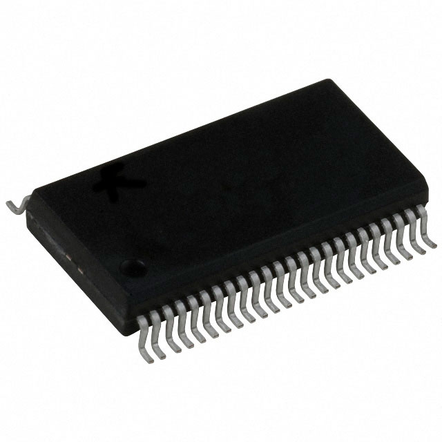
SN75LVDS84ADGGR
ActiveFLATLINK™ TRANSMITTER
Deep-Dive with AI
Search across all available documentation for this part.
SN75LVDS84ADGGR
ActiveFLATLINK™ TRANSMITTER
Deep-Dive with AI
Technical Specifications
Parameters and characteristics commom to parts in this series
| Specification | SN75LVDS84ADGGR | 75LVDS84 Series |
|---|---|---|
| Mounting Type | Surface Mount | Surface Mount |
| Number of Drivers/Receivers [custom] | 0 | 0 |
| Number of Drivers/Receivers [custom] | 4 | 4 |
| Operating Temperature [Max] | 70 ░C | 70 ░C |
| Operating Temperature [Min] | 0 °C | 0 °C |
| Package / Case | 48-TFSOP | 48-TFSOP |
| Package / Case | 0.24 in | 0.24 in |
| Package / Case [y] | 6.1 mm | 6.1 mm |
| Protocol | LVDS | LVDS |
| Supplier Device Package | 48-TSSOP | 48-TSSOP |
| Type | Driver | Driver |
| Voltage - Supply [Max] | 3.6 V | 3.6 V |
| Voltage - Supply [Min] | 3 V | 3 V |
Pricing
Prices provided here are for design reference only. For realtime values and availability, please visit the distributors directly
75LVDS84 Series
IC DRIVER 4/0 48TSSOP
| Part | Voltage - Supply [Max] | Voltage - Supply [Min] | Package / Case [y] | Package / Case | Package / Case | Type | Number of Drivers/Receivers [custom] | Number of Drivers/Receivers [custom] | Protocol | Operating Temperature [Max] | Operating Temperature [Min] | Mounting Type | Supplier Device Package |
|---|---|---|---|---|---|---|---|---|---|---|---|---|---|
3.6 V | 3 V | 6.1 mm | 48-TFSOP | 0.24 in | Driver | 0 | 4 | LVDS | 70 ░C | 0 °C | Surface Mount | 48-TSSOP | |
Texas Instruments SN75LVDS84ADGGRThe SN75LVDS84A and SN65LVDS84AQ FlatLink transmitters contains three 7-bit parallel-load serial-out shift registers, and four low-voltage differential signaling (LVDS) line drivers in a single integrated circuit. These functions allow 21 bits of single-ended LVTTL data to be synchronously transmitted over 3 balanced-pair conductors for receipt by a compatible receiver, such as the SN75LVDS82 or SN75LVDS86/86A.
When transmitting, data bits D0 - D20 are each loaded into registers of the 'LVDS84A upon the falling edge. The internal PLL is frequency-locked to CLKIN and then used to unload the data registers in 7-bit slices. The three serial streams and a phase-locked clock (CLKOUT) are then output to LVDS output drivers. The frequency of CLKOUT is the same as the input clock, CLKIN.
The 'LVDS84A requires no external components and little or no control. The data bus appears the same at the input to the transmitter and output of the receiver with the data transmission transparent to the user(s). The only user intervention is the possible use of the shutdown/clear (SHTDN\) active-low input to inhibit the clock and shut off the LVDS output drivers for lower power consumption. A low-level on this signal clears all internal registers to a low level.
The SN75LVDS84A is characterized for operation over ambient free-air temperatures of 0°C to 70°C. The SN65LVDS84AQ is characterized for operation over the full Automotive temperature range of -40°C to 125°C.
The SN75LVDS84A and SN65LVDS84AQ FlatLink transmitters contains three 7-bit parallel-load serial-out shift registers, and four low-voltage differential signaling (LVDS) line drivers in a single integrated circuit. These functions allow 21 bits of single-ended LVTTL data to be synchronously transmitted over 3 balanced-pair conductors for receipt by a compatible receiver, such as the SN75LVDS82 or SN75LVDS86/86A.
When transmitting, data bits D0 - D20 are each loaded into registers of the 'LVDS84A upon the falling edge. The internal PLL is frequency-locked to CLKIN and then used to unload the data registers in 7-bit slices. The three serial streams and a phase-locked clock (CLKOUT) are then output to LVDS output drivers. The frequency of CLKOUT is the same as the input clock, CLKIN.
The 'LVDS84A requires no external components and little or no control. The data bus appears the same at the input to the transmitter and output of the receiver with the data transmission transparent to the user(s). The only user intervention is the possible use of the shutdown/clear (SHTDN\) active-low input to inhibit the clock and shut off the LVDS output drivers for lower power consumption. A low-level on this signal clears all internal registers to a low level.
The SN75LVDS84A is characterized for operation over ambient free-air temperatures of 0°C to 70°C. The SN65LVDS84AQ is characterized for operation over the full Automotive temperature range of -40°C to 125°C. | 3.6 V | 3 V | 6.1 mm | 48-TFSOP | 0.24 in | Driver | 0 | 4 | LVDS | 70 ░C | 0 °C | Surface Mount | 48-TSSOP |
3.6 V | 3 V | 6.1 mm | 48-TFSOP | 0.24 in | Driver | 0 | 4 | LVDS | 70 ░C | 0 °C | Surface Mount | 48-TSSOP | |
Texas Instruments SN75LVDS84DGGRThe SN75LVDS84 FlatLink™ transmitter contains three 7-bit parallel-load serial-out shift registers, a 7× clock synthesizer, and four low-voltage differential signaling (LVDS) line drivers in a single integrated circuit. These functions allow 21 bits of single-ended low-voltage TTL (LVTTL) data to be synchronously transmitted over three balanced-pair conductors for receipt by a compatible receiver, such as the SN75LVDS82 or SN75LVDS86.
When transmitting, data bits D0–D20 are each loaded into registers of the SN75LVDS84 on the falling edge of the input clock signal (CLKIN). The frequency of CLKIN is multiplied seven times and then used to unload the data registers in 7-bit slices and serially. The three serial streams and a phase-locked clock (CLKOUT) are then output to LVDS output drivers. The frequency of CLKOUT is the same as the input clock, CLKIN.
The SN75LVDS84 requires no external components and little or no control. The data bus appears the same at the input to the transmitter and output of the receiver with the data transmission transparent to the user(s). The only possible user intervention is the use of the shutdown/clear (SHTDN) active-low input to inhibit the clock and shut off the LVDS output drivers for lower power consumption. A low level on this signal clears all internal registers to a low level.
The SN75LVDS84 is characterized for operation over ambient free-air temperatures of 0°C to 70°C.
The SN75LVDS84 FlatLink™ transmitter contains three 7-bit parallel-load serial-out shift registers, a 7× clock synthesizer, and four low-voltage differential signaling (LVDS) line drivers in a single integrated circuit. These functions allow 21 bits of single-ended low-voltage TTL (LVTTL) data to be synchronously transmitted over three balanced-pair conductors for receipt by a compatible receiver, such as the SN75LVDS82 or SN75LVDS86.
When transmitting, data bits D0–D20 are each loaded into registers of the SN75LVDS84 on the falling edge of the input clock signal (CLKIN). The frequency of CLKIN is multiplied seven times and then used to unload the data registers in 7-bit slices and serially. The three serial streams and a phase-locked clock (CLKOUT) are then output to LVDS output drivers. The frequency of CLKOUT is the same as the input clock, CLKIN.
The SN75LVDS84 requires no external components and little or no control. The data bus appears the same at the input to the transmitter and output of the receiver with the data transmission transparent to the user(s). The only possible user intervention is the use of the shutdown/clear (SHTDN) active-low input to inhibit the clock and shut off the LVDS output drivers for lower power consumption. A low level on this signal clears all internal registers to a low level.
The SN75LVDS84 is characterized for operation over ambient free-air temperatures of 0°C to 70°C. | 3.6 V | 3 V | 6.1 mm | 48-TFSOP | 0.24 in | Driver | 0 | 4 | LVDS | 70 ░C | 0 °C | Surface Mount | 48-TSSOP |
Texas Instruments SN75LVDS84DGGThe SN75LVDS84 FlatLink™ transmitter contains three 7-bit parallel-load serial-out shift registers, a 7× clock synthesizer, and four low-voltage differential signaling (LVDS) line drivers in a single integrated circuit. These functions allow 21 bits of single-ended low-voltage TTL (LVTTL) data to be synchronously transmitted over three balanced-pair conductors for receipt by a compatible receiver, such as the SN75LVDS82 or SN75LVDS86.
When transmitting, data bits D0–D20 are each loaded into registers of the SN75LVDS84 on the falling edge of the input clock signal (CLKIN). The frequency of CLKIN is multiplied seven times and then used to unload the data registers in 7-bit slices and serially. The three serial streams and a phase-locked clock (CLKOUT) are then output to LVDS output drivers. The frequency of CLKOUT is the same as the input clock, CLKIN.
The SN75LVDS84 requires no external components and little or no control. The data bus appears the same at the input to the transmitter and output of the receiver with the data transmission transparent to the user(s). The only possible user intervention is the use of the shutdown/clear (SHTDN) active-low input to inhibit the clock and shut off the LVDS output drivers for lower power consumption. A low level on this signal clears all internal registers to a low level.
The SN75LVDS84 is characterized for operation over ambient free-air temperatures of 0°C to 70°C.
The SN75LVDS84 FlatLink™ transmitter contains three 7-bit parallel-load serial-out shift registers, a 7× clock synthesizer, and four low-voltage differential signaling (LVDS) line drivers in a single integrated circuit. These functions allow 21 bits of single-ended low-voltage TTL (LVTTL) data to be synchronously transmitted over three balanced-pair conductors for receipt by a compatible receiver, such as the SN75LVDS82 or SN75LVDS86.
When transmitting, data bits D0–D20 are each loaded into registers of the SN75LVDS84 on the falling edge of the input clock signal (CLKIN). The frequency of CLKIN is multiplied seven times and then used to unload the data registers in 7-bit slices and serially. The three serial streams and a phase-locked clock (CLKOUT) are then output to LVDS output drivers. The frequency of CLKOUT is the same as the input clock, CLKIN.
The SN75LVDS84 requires no external components and little or no control. The data bus appears the same at the input to the transmitter and output of the receiver with the data transmission transparent to the user(s). The only possible user intervention is the use of the shutdown/clear (SHTDN) active-low input to inhibit the clock and shut off the LVDS output drivers for lower power consumption. A low level on this signal clears all internal registers to a low level.
The SN75LVDS84 is characterized for operation over ambient free-air temperatures of 0°C to 70°C. | 3.6 V | 3 V | 6.1 mm | 48-TFSOP | 0.24 in | Driver | 0 | 4 | LVDS | 70 ░C | 0 °C | Surface Mount | 48-TSSOP |
Texas Instruments SN75LVDS84ADGGThe SN75LVDS84A and SN65LVDS84AQ FlatLink transmitters contains three 7-bit parallel-load serial-out shift registers, and four low-voltage differential signaling (LVDS) line drivers in a single integrated circuit. These functions allow 21 bits of single-ended LVTTL data to be synchronously transmitted over 3 balanced-pair conductors for receipt by a compatible receiver, such as the SN75LVDS82 or SN75LVDS86/86A.
When transmitting, data bits D0 - D20 are each loaded into registers of the 'LVDS84A upon the falling edge. The internal PLL is frequency-locked to CLKIN and then used to unload the data registers in 7-bit slices. The three serial streams and a phase-locked clock (CLKOUT) are then output to LVDS output drivers. The frequency of CLKOUT is the same as the input clock, CLKIN.
The 'LVDS84A requires no external components and little or no control. The data bus appears the same at the input to the transmitter and output of the receiver with the data transmission transparent to the user(s). The only user intervention is the possible use of the shutdown/clear (SHTDN\) active-low input to inhibit the clock and shut off the LVDS output drivers for lower power consumption. A low-level on this signal clears all internal registers to a low level.
The SN75LVDS84A is characterized for operation over ambient free-air temperatures of 0°C to 70°C. The SN65LVDS84AQ is characterized for operation over the full Automotive temperature range of -40°C to 125°C.
The SN75LVDS84A and SN65LVDS84AQ FlatLink transmitters contains three 7-bit parallel-load serial-out shift registers, and four low-voltage differential signaling (LVDS) line drivers in a single integrated circuit. These functions allow 21 bits of single-ended LVTTL data to be synchronously transmitted over 3 balanced-pair conductors for receipt by a compatible receiver, such as the SN75LVDS82 or SN75LVDS86/86A.
When transmitting, data bits D0 - D20 are each loaded into registers of the 'LVDS84A upon the falling edge. The internal PLL is frequency-locked to CLKIN and then used to unload the data registers in 7-bit slices. The three serial streams and a phase-locked clock (CLKOUT) are then output to LVDS output drivers. The frequency of CLKOUT is the same as the input clock, CLKIN.
The 'LVDS84A requires no external components and little or no control. The data bus appears the same at the input to the transmitter and output of the receiver with the data transmission transparent to the user(s). The only user intervention is the possible use of the shutdown/clear (SHTDN\) active-low input to inhibit the clock and shut off the LVDS output drivers for lower power consumption. A low-level on this signal clears all internal registers to a low level.
The SN75LVDS84A is characterized for operation over ambient free-air temperatures of 0°C to 70°C. The SN65LVDS84AQ is characterized for operation over the full Automotive temperature range of -40°C to 125°C. | 3.6 V | 3 V | 6.1 mm | 48-TFSOP | 0.24 in | Driver | 0 | 4 | LVDS | 70 ░C | 0 °C | Surface Mount | 48-TSSOP |
Description
General part information
75LVDS84 Series
The SN75LVDS84A and SN65LVDS84AQ FlatLink transmitters contains three 7-bit parallel-load serial-out shift registers, and four low-voltage differential signaling (LVDS) line drivers in a single integrated circuit. These functions allow 21 bits of single-ended LVTTL data to be synchronously transmitted over 3 balanced-pair conductors for receipt by a compatible receiver, such as the SN75LVDS82 or SN75LVDS86/86A.
When transmitting, data bits D0 - D20 are each loaded into registers of the 'LVDS84A upon the falling edge. The internal PLL is frequency-locked to CLKIN and then used to unload the data registers in 7-bit slices. The three serial streams and a phase-locked clock (CLKOUT) are then output to LVDS output drivers. The frequency of CLKOUT is the same as the input clock, CLKIN.
The 'LVDS84A requires no external components and little or no control. The data bus appears the same at the input to the transmitter and output of the receiver with the data transmission transparent to the user(s). The only user intervention is the possible use of the shutdown/clear (SHTDN\) active-low input to inhibit the clock and shut off the LVDS output drivers for lower power consumption. A low-level on this signal clears all internal registers to a low level.
Documents
Technical documentation and resources